
Probably not worth talking about the importance of checking the radio components before installation. Basically, of course, this applies to soldered elements that were in work, although in critical cases, it does not hurt to make sure new ones are working. Recently, it has become possible inexpensively, or even completely free, to replenish your bins with radioelements from devices potentially sent to landfill. Partly due to the growth of well-being of the average layman, partly due to the rapid development e appliances, appliances are increasingly being sent to the scrap, household appliances are obsolete “morally” - long live the advertising business and snobbery of citizens. You can walk through your friends about the subject - rummaging around in their rubbish in the attics, basements, cottages, you can advertise in the newspaper, sort of, "I’ll get it for a symbolic price," and finally throw a cry among friends.
Dismantling - soldering of electronic components, from torture, during the predominance of volumetric installation (sometimes they even used the welding of leads of individual elements), turned into a quite simple, but rather dreary occupation in the era of the spread in the technique of conventional printed wiring with output elements. Now, with the predominance of surface mounting elements, their soldering, just the same pleasure - you only need a building hair dryer or a halogen spotlight and a paint brush. Dismantling by disassembling, but with the identification of SMD elements, this is just the trouble - tiny, with a match head radio components with markings that differ from different manufacturers. Moreover, on some types of elements in the SMD version, often, the marking is missing as such. For example, capacitors or small (in 0805 cases) resistors. Resistors, of course, you can measure with any tester, but what about the rest?
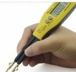
There are special, tweezers-like testers that focus on the definition of dual pin SMD. I don’t have this myself, but their extreme convenience seems to be, however, they can be determined only by a very limited set of elements - a diode-resistor-capacitor.
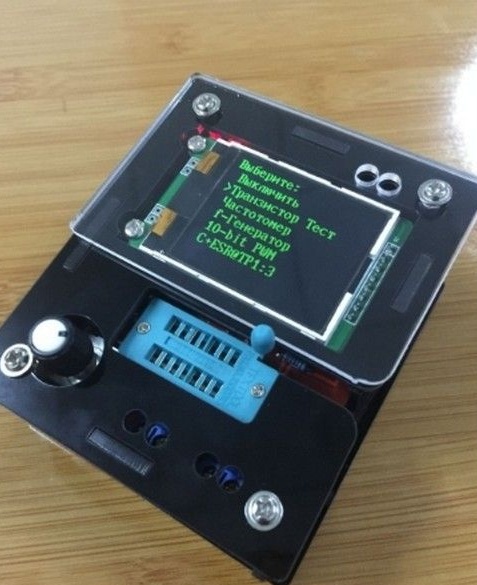
There are also testers who can determine a significantly wider range of elements and their parameters. Recently, such devices have appeared on sale at the well-known Aliexpress.There are several options, differ in features and additional functions. A relatively simple device (), which can only determine components, was purchased.
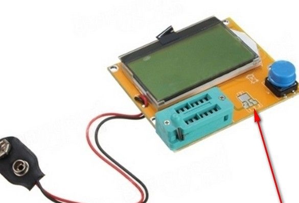
The findings of the tested elements are clamped in the contact block with "zero force", legless SMD are applied to a specially organized printing pad, shaped to conveniently connect all the main types of cases.
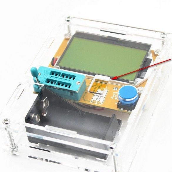
The device in the form of a housingless module came out half cheaper. And the corps, admittedly, was not particularly impressed - that's more about that.
There are similar devices equipped with a housing or housing purchased separately and mounted independently. Take a look at them.

Well, this is the most “cultural” option, the set includes remote probes with small clamps, for SMD it’s not very adapted - a printing pad, right word, which is much more convenient. But it looks nice, this does not take away.
Let's move on to simplified cases. Rather, it’s some kind of enclosures, their IP, it seems, is negative, and the price, for all its unpretentiousness, is comparable to the price of the device.
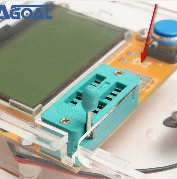
But the most unpleasant thing is that the case blocks access to the contact area on the printed circuit board and SMD is now not to be measured.
The case for another model of a similar device has a window for accessing the “SMD platform”, but the distance to it is great and it is categorically not convenient to use - it’s on your mind that the piggy bank immediately comes in — when many details come inside, through a small hole, you can take it apart and shake everything, br-r.
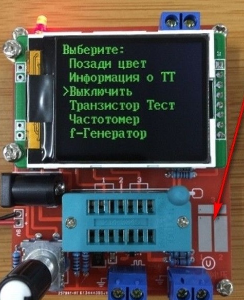
The contact pads of a similar device also turn out to be buried when the module is installed in the housing intended for it.
Well, you have to move your brains.
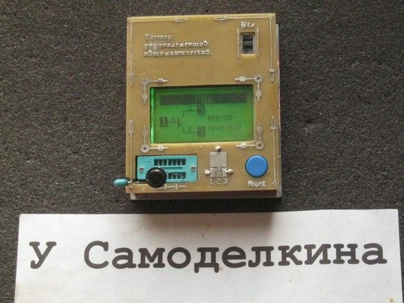
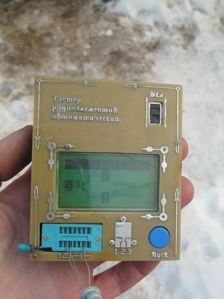
The device definitely needs a housing - the wiring to the battery block and the fragile glass of the screen make measurements, frankly, not too convenient. Moreover, sometimes the tasks of “field” electrical measurements arise, well, say, measuring the capacity of an isolated mast relative to the ground, and just moving the device from place to place requires some caution. It doesn’t matter.
Understandably, the SMD pad should be outside. The evolution of the design solution was something like this - a printing pad fixed to the front of a textolite (plastic) case, the front panel itself is entirely of foil fiberglass with an etched pad for SMD, and finally, walk like that for a walk, the whole case soldered from foil material. By the way, at a time when the foil textolite was sold in Hefty Technique stores as hefty sheets, like plywood in construction stores, the cases made of it were very popular among radio amateurs. And to say that - it is easy to process, the walls are connected with the help of native and familiar soldering, the case is lightweight, shielded, easy to paint. Now, when for each piece they tear in three roads, and there are ready-made cases on sale, the practice of making such home-made ones is leaving.
So (rubbing our hands) let's get started.
What was needed in the manufacture.
Tools, devices.
A set of small bench tools, needle files, a regular jigsaw on wood and jewelry. Something for drilling holes, including small "printed" (~ 0.8 mm). A set of tools for radio installation, a soldering iron of low power and more powerful, watt sort of 60, for structural soldering. Belonging to them. Scalpel. Multimeter for continuity chains. Access to a computer with a printer. Some little things for special photo printing - a lightproof drying box, device for UV illumination, stopwatch, containers and chemicals for development and etching.
Materials
In addition to the most purchased module, I needed a double-sided foil-coated fiberglass, transparent film for printing on a printer, a piece of plexiglass for a window, transparent adhesive tape, reagents for making a printed circuit board - photoresist varnish, NaOH (can be replaced with a pipe cleaner, for example, “Mole”, it contains this alkali), ferric chloride for etching copper (any of the known compositions for etching).
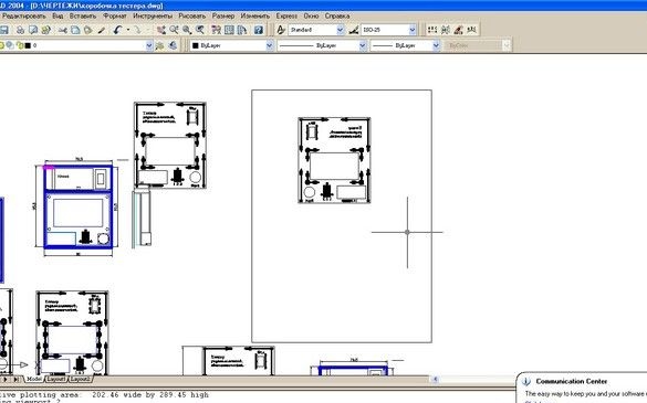
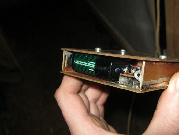
The first thing, of course, is to draw. General layout, front panel.Since it’s still possible to transfer the drawing and etch, I could not resist and added “ruffles”, since I didn’t even have to draw them - I took some elements ready for frequency meter and adjusted to the desired size. I decided to place the battery compartment over the device, it seemed a little more convenient. Yes, it was decided to introduce a power switch in the design, so that after measurements do not get involved pulling out the battery. A switch was required, such, such ... (by moving his fingers in the air), so that it would not turn on independently, say, in a pocket. There was a switch from an old computer power supply.
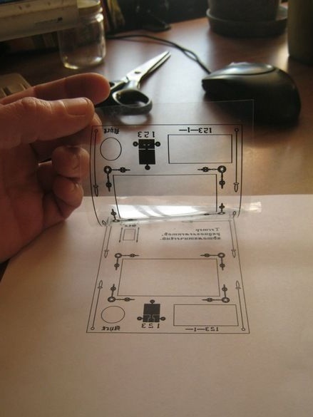
After several successive iterations with printing and trying on the front panel, the drawing was ready, a photo template was printed for transferring the image of contact photo printing.
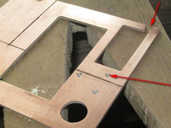
In terms of size, the remaining elements of the case were cut and installation began.
But the lid of the battery compartment, I'm really proud. Rate it! The protrusion cover is inserted into the corresponding groove on the one hand and fixed in place with a short M3 screw, on the other. The groove and the corresponding spike were cut out with a jewelry jigsaw - it has the finest files, the nut is simply soldered in the right place.
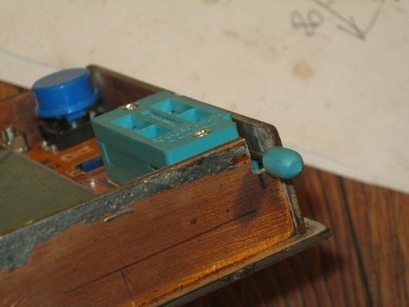
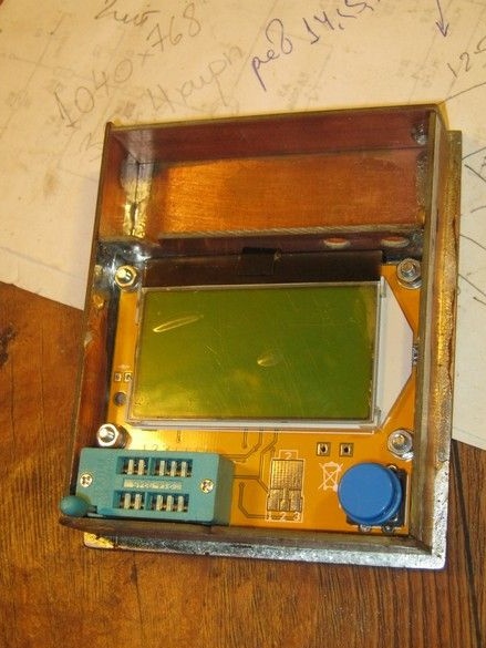
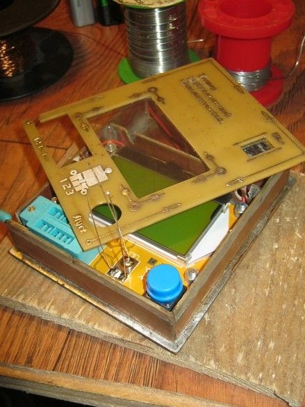
Everything, the module itself is set to death in a relying compartment. Nuts, washers, stoppers, everything is like people have.

The sketch of the upper front panel was refined for the last time in place, adjustments have been made, you can begin to manufacture. Making the top cap - method "home"Printed circuit boards. Who owns what (LUTs, photoresist, magical trackfinder, finally). Here, an aerosol photoresist and contact photo printing were applied. In the ultraviolet light. I screwed up a little with a photo template, but it wasn’t very much a remake, I left it like that - it’s important here that contact pads are not closed, the rest is just for beauty.
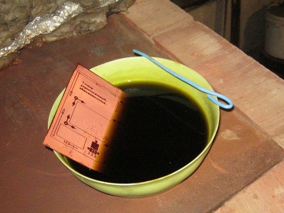
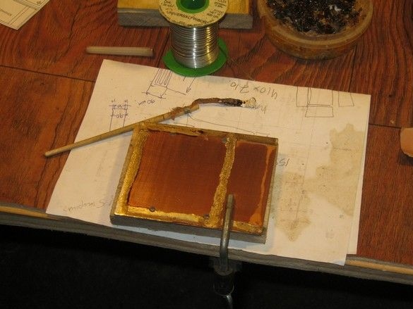
Etched the “scarf” in a textbook - in a solution of ferric chloride, previously protecting the back foil side of the workpiece, with two layers of nitrolac. Metallization is there, we still need.
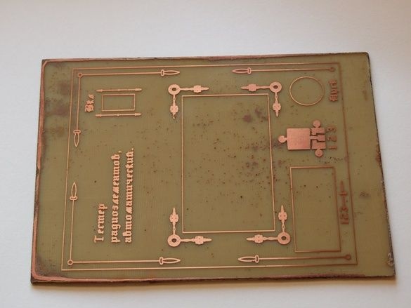
A number of minor defects are visible - the "starry sky" and low resolution. The result of a not-so-successful experiment with photo masks.
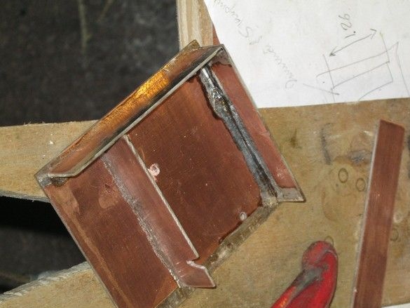
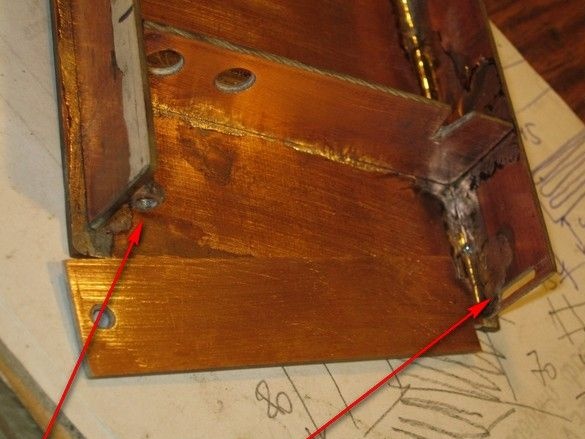
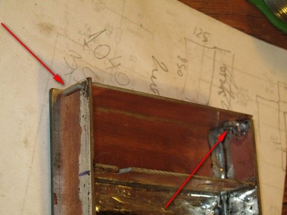
The board was sawn with a hacksaw for metal, the internal openings with a jigsaw for wood, the edges were filed and sanded. Recess for the clamping lever, sawn with a special file with a diameter of about 5 mm, for sharpening the saw chains of chainsaws. So that the wires that we will pass through the top panel and solder to the pads for SMD elements are not closed by foil on the back of the panel, the holes are countersinked.
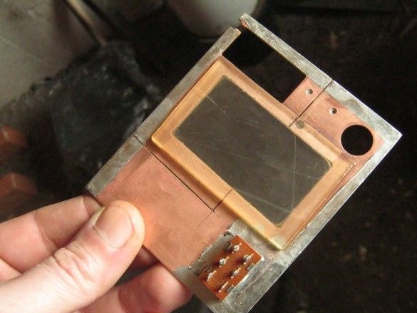
I sawed off the protruding ears at the switch and soldered it to death. Epoxy, pasted a window.
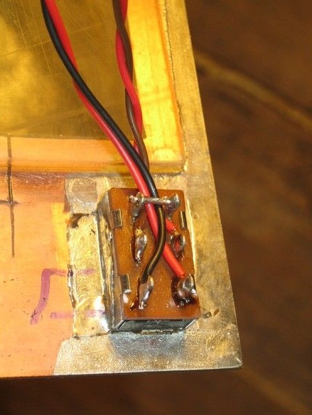
A free contact group is used as a wire fastener - standard ones from the battery terminal, frankly, not important - rather rough insulation with a very thin conductive core, such wires are easily broken off at the soldering point.
Connecting the main highlight of the design - the remote contact pad for housing elements. Pieces of tinned wire are soldered to the standard sites, and passed through the corresponding holes in the top cover. Then, after the final assembly of the case, the conductors are shortened and sealed.
The leads are connected to the circuit breaker in such a way that the wires from the battery block are soldered to the contacts closest to the “output” - in case of a break, it will be possible to reach the soldering iron without disassembling (soldering the case).