
This article will discuss how to make electronic devices on a silicone base. This work was presented by a group of Belgian scientists from the University of Hasselt to familiarize everyone. Various electronic components LEDs, microcontrollers, input and output devices, power supplies, etc. can be integrated into silicone devices. combined into one silicone, bendable and stretchable housing.
The device presented in this article is more for educational purposes with the very process of manufacturing such circuits.
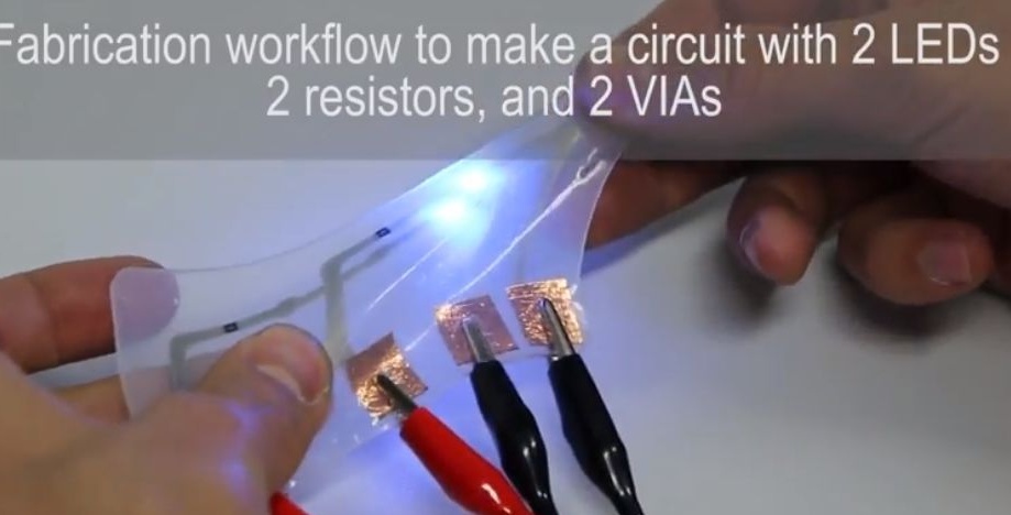
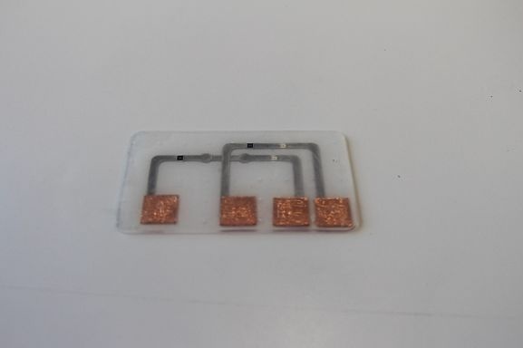
Let's watch a short video.
As you can see, the device is stretched, compressed and continues to function properly. Of course, these technologies are already used in industry, but such devices can be manufactured and do it yourself.
The whole process takes no more than 2 hours, if you have all the necessary tools and use silicone with a cure of 15 minutes.
Despite the fact that the design is quite simple, this technology is suitable for many types of SMD components and any number of layers.
At the end of the article, several links will be given to a more detailed description of this technology, as well as a video of the manufacturing process of such devices.
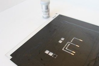
Tools and materials:
-Laser type apparatus
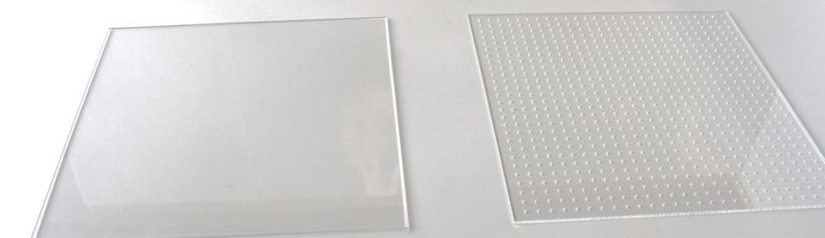
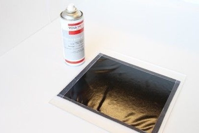
- Acrylic 3 mm (2 squares 280x280 mm);
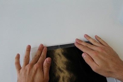
-Black vinyl sticker (you need 4 squares about 260x260 mm)
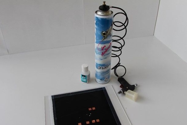
- Spery for molds (or);
-Pencil;
- Soft construction roller;
-Silicone primer (or);
- Two-component silicone (or);
-Two LEDs;
-Two 100 Ohm resistors;
- Copper, aluminum tape or foil;
-Scotch;
-Device with adjustable blade height (see step 5);
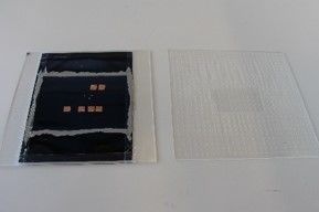
Step One: Acrylic
First you need to prepare two plates of acrylic. The size of the plates for this bracelet is 280 * 280 mm. In one plate, you need to make holes over the entire surface.
Step Two: Lower Plate
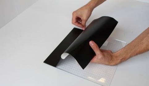
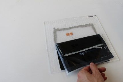
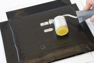
A layer of mold fluid is sprayed onto the acrylic plate (without holes). Then a vinyl film is cut, slightly smaller than the plate, and glued to the plate. The film should lie on the plate evenly, without wrinkles. The edges of the film are fixed with tape. Then the film is sprayed into, in two layers, a spray for molds. Using a cutter, a device diagram is applied. No need to cut the film, just a drawing. Then sprayed in two layers.
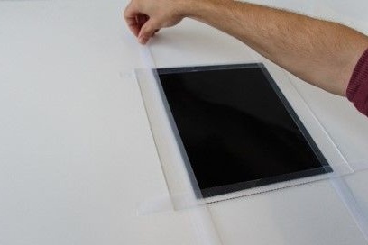
Step Two: Preparing the Top Plate
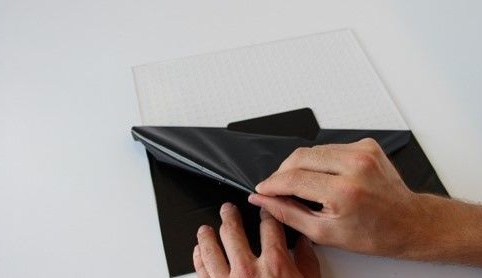
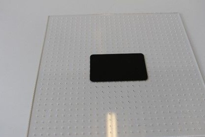
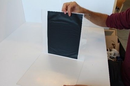
Now you need to prepare the top plate. Sticks a film on the top plate. Using a cutter, cuts the film in the center according to the size of the device + 5 mm on each side. Removes excess film.
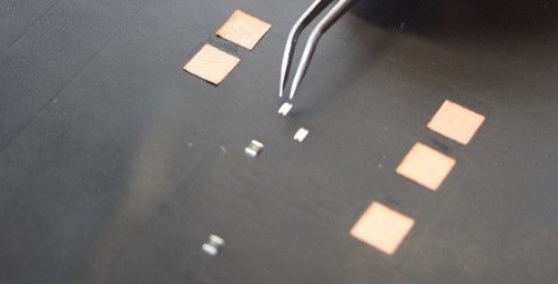
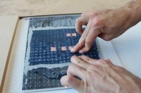
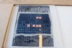
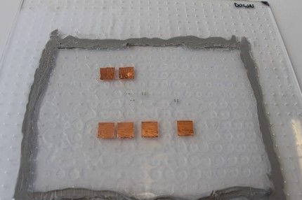
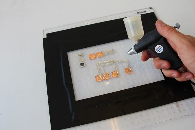
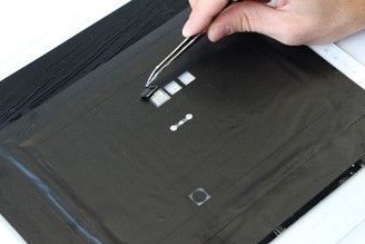
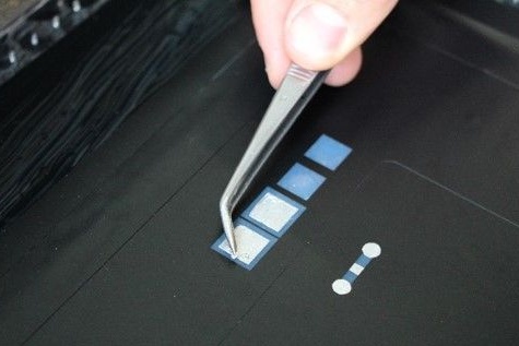
Step Three: Install Electronic Components
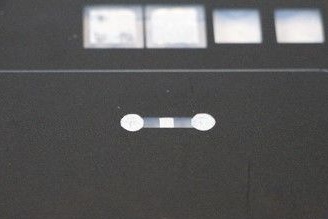
Now, on the lower layer, it is necessary, according to the diagram, to place the electronics. In this case, these are LEDs, resistors, and contacts. For such devices, you must use SMD components. Size 2010 is recommended. The distance between the contacts should be at least 0.8 mm. SMD components are fixed on the film with the contacts down.
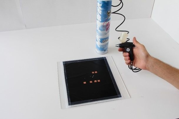
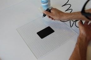
Step Four: Primer
A primer must be applied to the bottom plate with the installed electronic components.
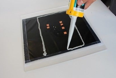
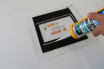
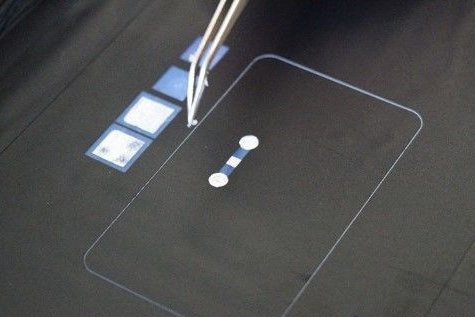
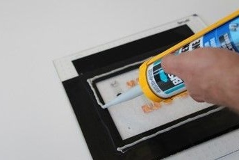
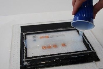
Step Five: First Layer
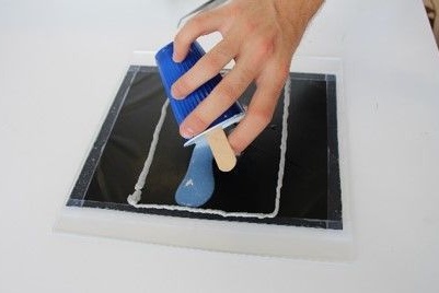
Then you can begin to fill the first layer. Along the perimeter of the mold to be poured, it is necessary to make a side made of building silicone. Then mix the two silicone components and pour into the mold. The layer thickness should be 0.3 mm larger than the thickest electronic component. In this case, it is 1 mm. This thickness is achieved using a special device with adjustable clearance between the blade and the surface. After the formation of the first layer, it is necessary to wait until it dries.
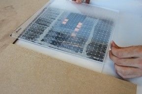
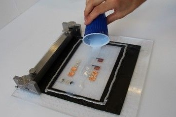
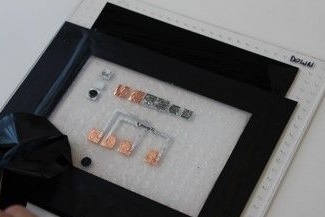
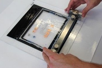
Step Six: Top Plate
Now you need to install a plate with holes on top, turn everything around and remove the bottom plate and film. To do this, the following actions are performed:
1. A primer is applied to the top plate.
2. The vinyl film is removed.
3. Divorced two-component silicone.
4. Apply silicone to the hardened form.
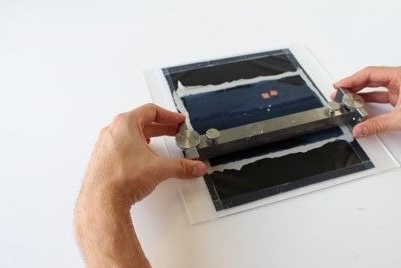
5. On top of the first sheet, a second with holes is installed
Next, you need to combine the two sheets exactly one above the other and press on the sheet so that the silicone begins to squeeze through the holes. Align again and wait for the silicone to dry.
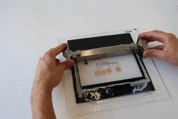
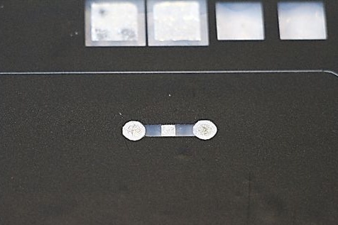
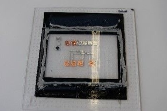
Seventh step: removing the bottom plate
Next, turn the plates over and carefully remove the bottom plate and film. If necessary, you can use a knife. After removing the film, you need to check with a multimeter that silicone has not got on the contacts of the electronic components.
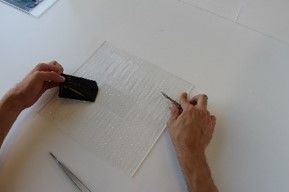
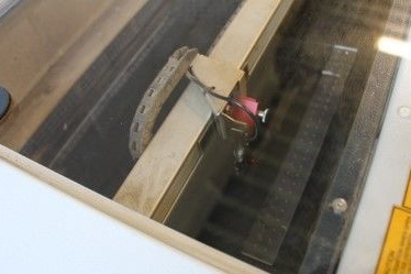
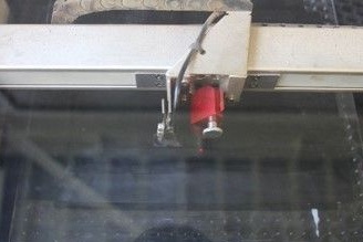
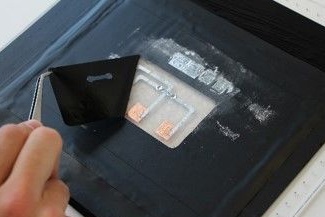
Step Eight: Laser Cutting
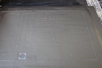
Next, you need to stick a new film on the surface, put everything in the cutter and cut the tracks. If the layers are not offset, then the tracks will be placed exactly according to the scheme. Otherwise, an adjustment is necessary.
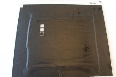
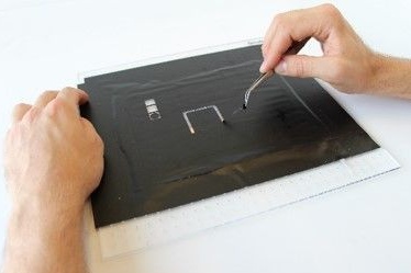
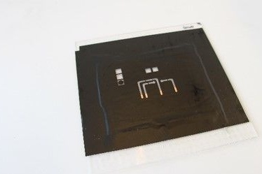
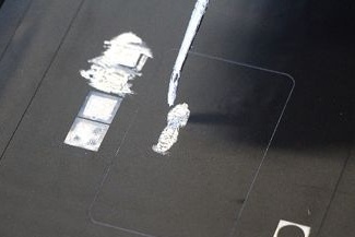
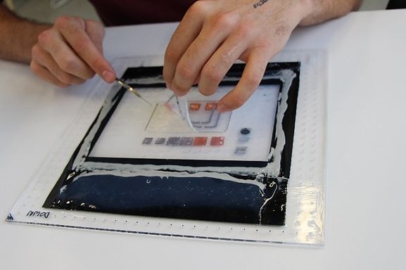
Step Nine: Top Conductive Layer
It is necessary that the film fits snugly to the surface and the metal does not leak under it.
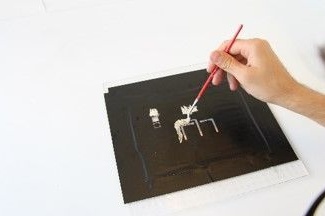
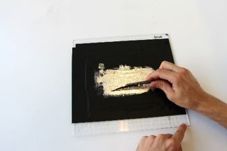
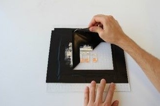
First you need to degrease the tracks with alcohol. Then, with a brush, apply liquid metal to the tracks and pads. With a soft roller, the metal rolls on the surface. The inner film is removed, then the outer one. Now you need to ring the tracks with a multimeter.
Step Ten: Second Silicone Layer
A primer is applied to the surface of the device.
After the primer dries, it is necessary to make a side, replace the silicone and place it on the surface. The operations are the same as in the previous steps. The most important layer thickness. The previous layer was 1 mm (LED 0.7 mm + 0.3 mm). A new layer is poured with a thickness of 0.5 mm to compensate for irregularities in the liquid metal. Those. the thickness of the two layers is 1.5 mm.
Step eleven: stencil for the second conductive layer
Further, the actions are repeated earlier.
The vinyl sticker is cut off and glued to the surface. Tracks are cut according to the pattern. Vinyl film is removed at the track locations.
Step twelve: connecting the conductive layers
Now you need to cut holes in the silicone between the layers on the cutter according to the diagram. After teething, the silicone is removed from the holes.
Step Thirteen: The Second Conductive Layer
The second layer is applied in the same way as the first. Degreasing, brushing, roller rolling and vinyl removal.If everything is done correctly, then the liquid metal through the holes should connect the two conductive layers.
Step Fourteen: The Last Silicone Layer
Now, according to the proven technology, the last silicone layer with a thickness of 0.5 mm is poured. Thus, the total thickness of the manufactured device will be only 2 mm.
Step Fifteen: Contacts
As previously mentioned, in such silicone devices you can insert batteries and other electronic components. This unit is powered by an external power source. To access the contacts, you need to cut out the contacts on the laser cutter and remove the silicone. Then you need to apply solder to the contacts.
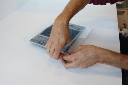
Step sixteen: removing the top plate
Since the primer was applied only on the edges to the top plate, the middle part should easily separate from the plate. You just need to cut the board along the contour and pry off one edge from the plate.
Now it remains to connect the device to a power source and check. If everything is done correctly, then such a circuit can withstand 1/2 tension without damaging the chain.
Links to fact-finding material provided by the author,,,.
Video on the manufacture of silicone electronic devices.