We survived - intramural monuments are already being erected on this microcircuit. The author of Instructables under the nickname YADUKRISHNAN K M assembled a functional analog of the 555 timer (KR1006VI1) on transistors and placed it in a huge case with legs, marking - everything is as it should be. On it you can collect the same circuits as on the regular 555 timer - it will work!
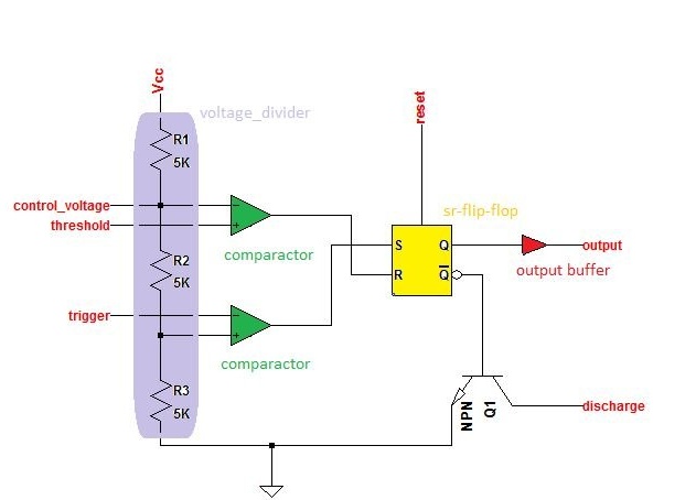
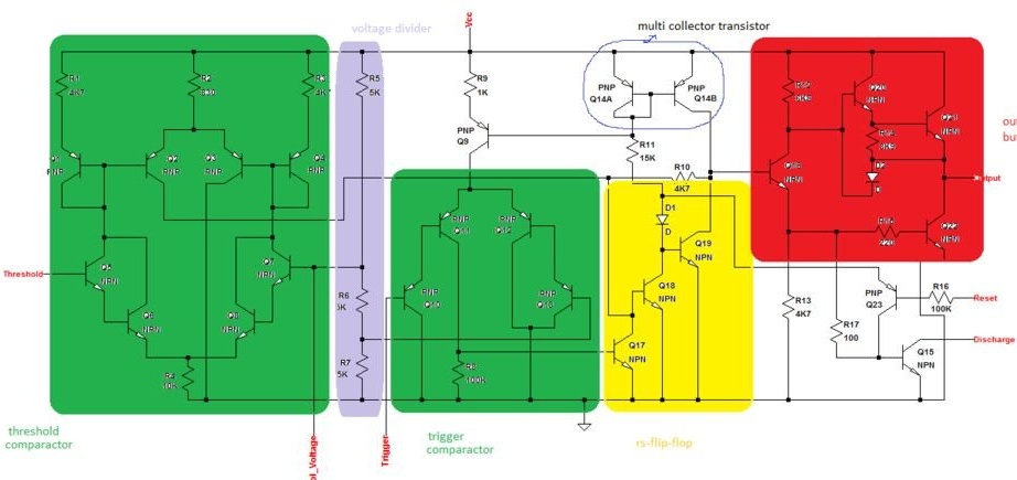
Compared, for example, with a microcontroller, this chip is designed simply. It consists of: a resistor divider, two comparators, an RS-flip-flop, as well as a transistor switch for receiving an open-collector output. In general, for a functional analogue, a huge cabinet is not required. There will be a device about the size of an audio cassette. But still, compared to a tiny crystal - impressive.
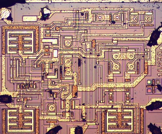
The crystal looks like this:
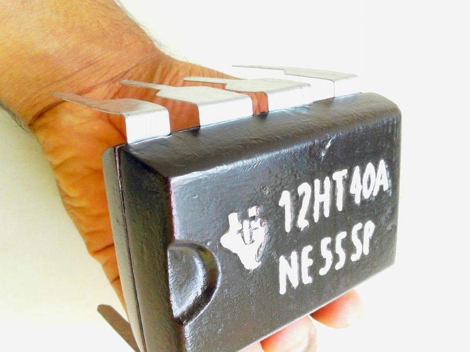
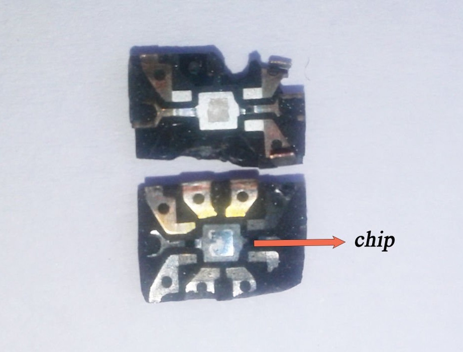
And here he is in the case, connected to the findings:
From the functional circuit to the electrical:
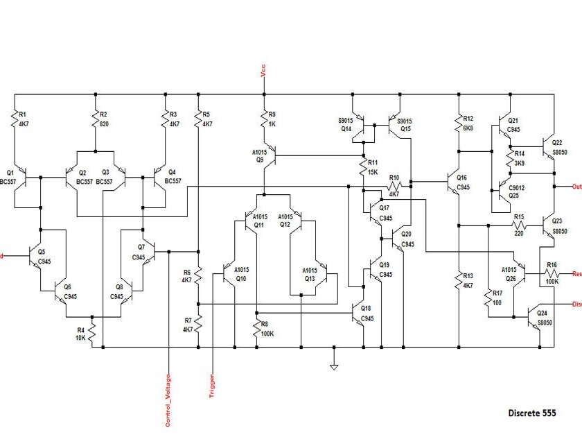
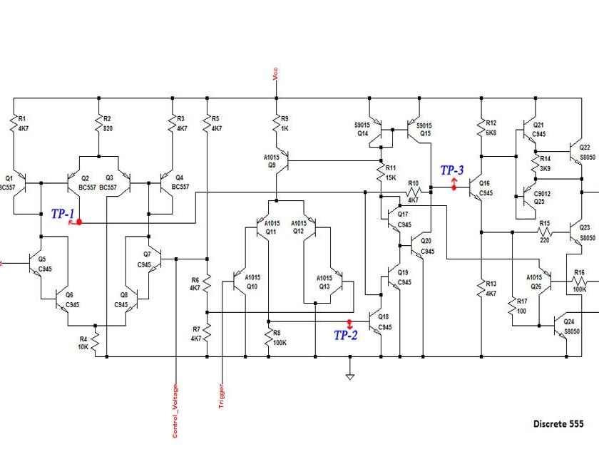
On its basis, the master developed his own scheme, according to which he will assemble a functional analogue. It indicates what types of transistors will be. Two diodes are replaced by transistors, each of which has a base connected to a collector:
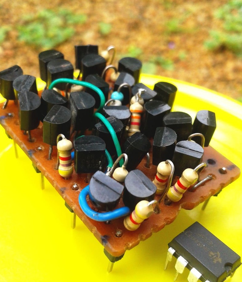
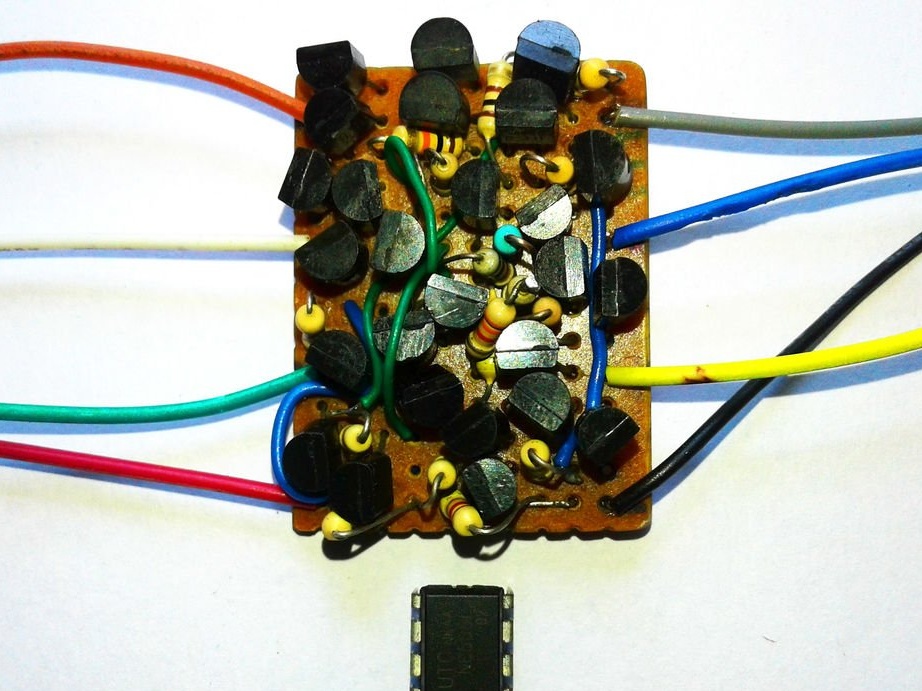
Even without the case, the resulting board looks gigantic compared to the microcircuit:
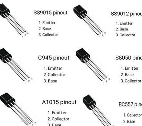
The following figure lists the types of transistors used in the circuit and their pinouts:
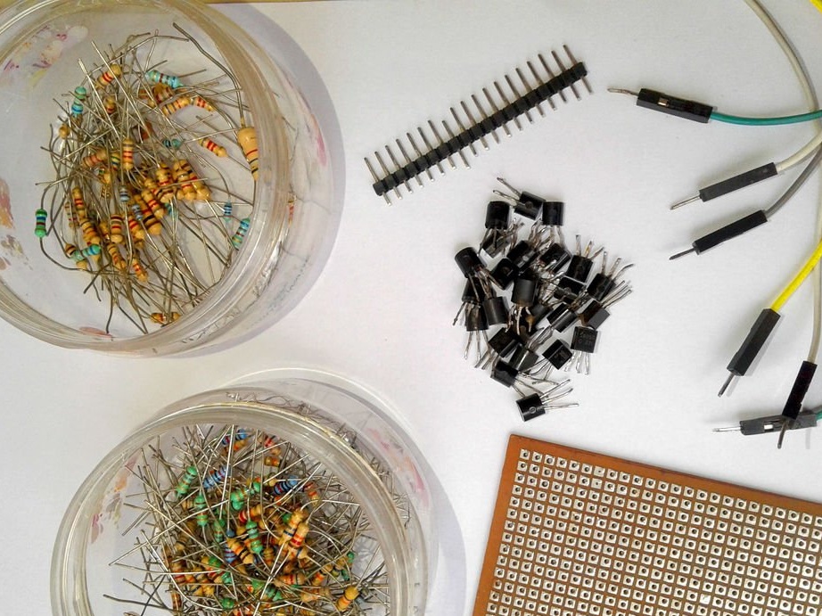
The transistors master soldered their old circuit boards, so they have such short conclusions. Resistors took new ones. I chose a breadboard, such as perfboard:
I took the necessary tools, consumables:
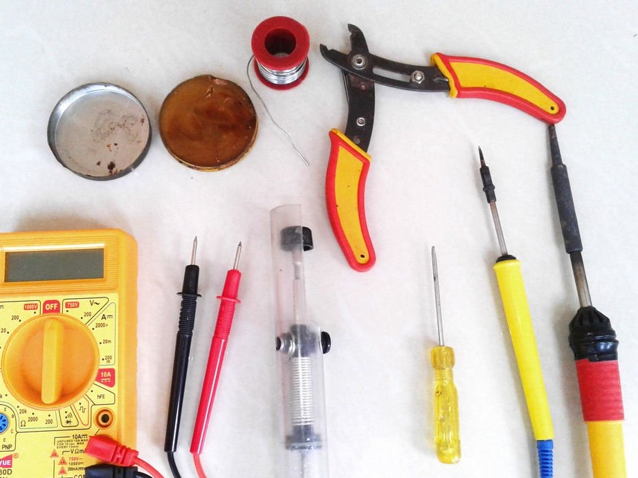
For soldering transistors, YADUKRISHNAN K M uses a standard desoldering pump:
In more detail, the methods of extracting are shown in the video:
In order not to overheat the transistors, they must be alternated during desoldering. One pin of one transistor was soldered, then one pin of another, third, etc. Then they returned to the first, soldered yet another conclusion, did the same with the second, and so on, until all the conclusions of all the transistors were soldered.
The soldered transistors the master checks with a multimeter in the diode test mode. Checking one transistor is like checking two diodes. If it is an N-P-N structure, the basic output when checking is equivalent to the connected anodes of the diodes, check this transistor like this:
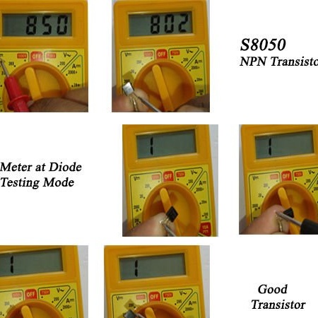
And if the structures are P-N-P, then the base pin is equivalent to the cathodes of the diodes connected together, such a transistor is checked differently:
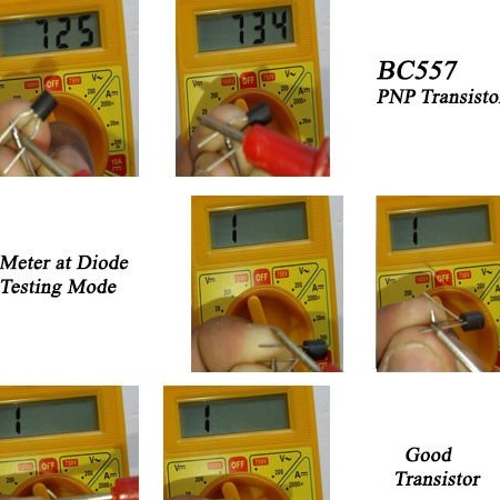
But it makes no sense to try to make a transistor of two diodes - it will not amplify.
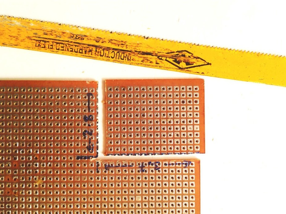
From a breadboard such as perfboard, the master cuts a 37x28 mm rectangle with a hacksaw:
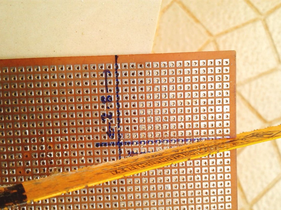
Attention, the board should NOT be made of fiberglass, otherwise the hands and respiratory organs should be protected during processing. And here is the result:
The master removes the bevels from the board with a file, cleans it of dust, and then begins to put the components into it:
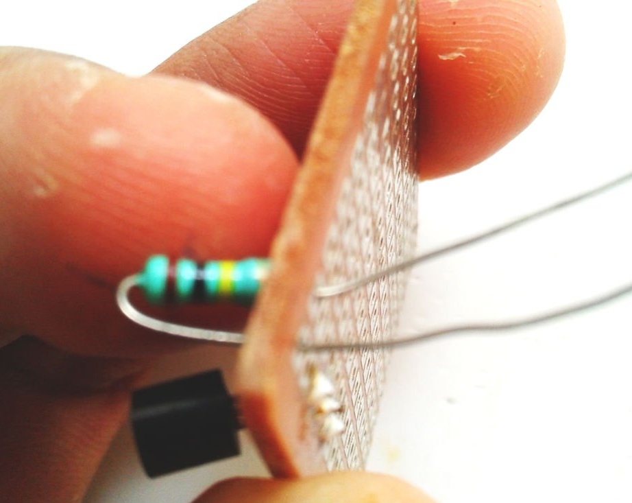
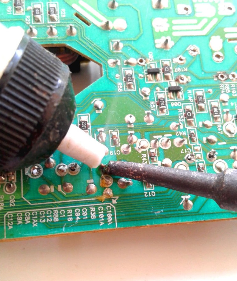
Solder them:
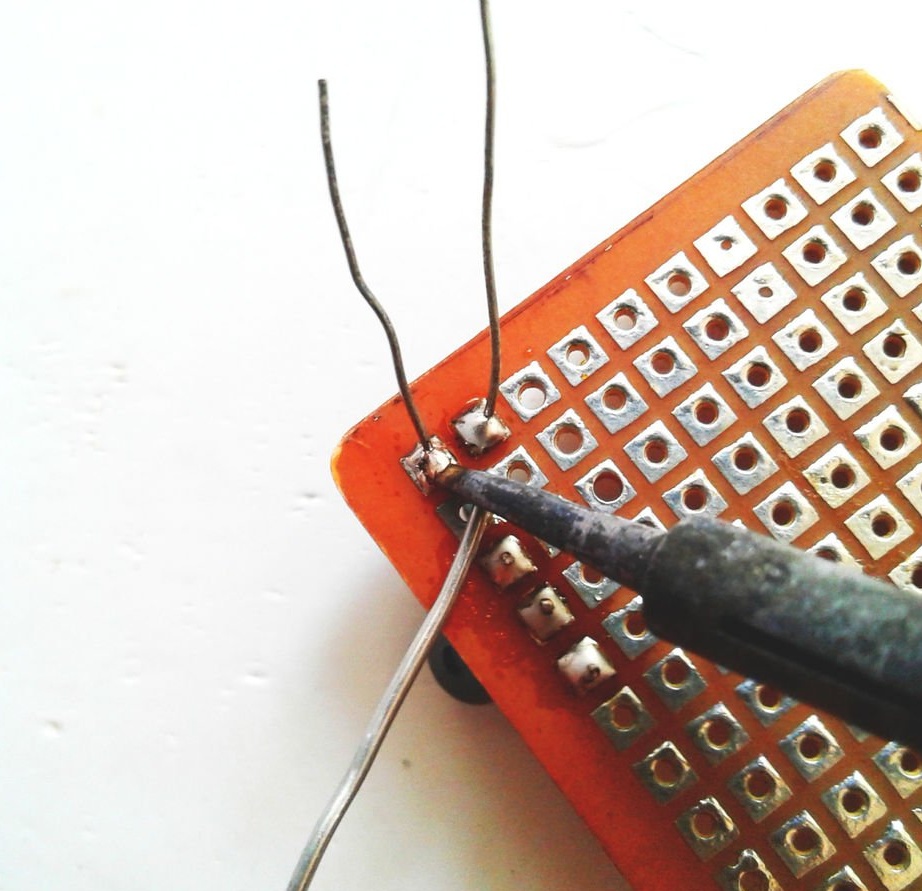
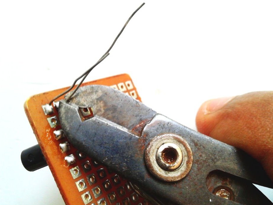
Since transistors are soldered from old boards, their conclusions are already short, but resistors must be bit off after soldering:
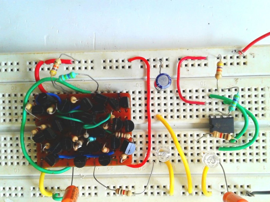
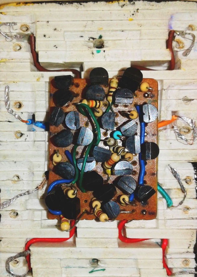
Soldering all the components, the master connects them with wires:
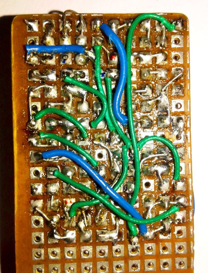
And solders those eight wires that will go to the huge conclusions:
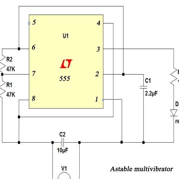
Next, you need a voltage source of 8 V. The consumed current of the device, if only power is supplied, should be about 10 mA. After making sure of this, the master puts a functional analog in the test bench, assembled according to this scheme:
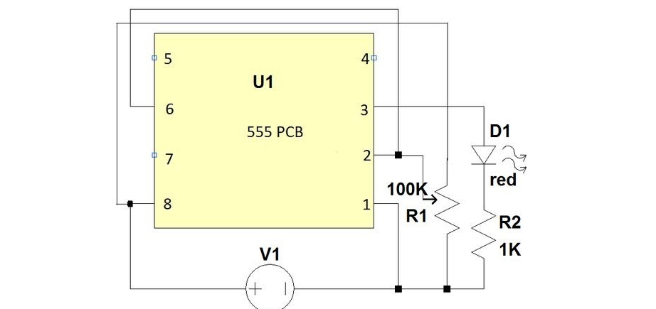
Rotating the variable resistor, it measures the voltages at the test points TP-1, TP-2 and TP-3:
At point TP-1, the voltage should be equal to 0.6 V, when the voltage removed from the variable resistor is more than 2/3 of the supply voltage, and when it is less, it should drop abruptly to 0 V.
At point TP-2, the voltage should be equal to 0.6 V, when the voltage removed from the variable resistor is less than 1/3 of the supply voltage, and when it is more, it should drop abruptly to 0.2 V.
At the point TP-3, hysteresis should be observed: gradually raise the voltage on the AC voltage slider to 2/3 of the supply voltage, the voltage at the test point jumps up to 1.44 V, gradually decreases up to 1/3 - drops down to 0 V.
If the results are incorrect, the corresponding comparators must be checked at the first and second points, and the RS-trigger at the third point. Having corrected everything with the power off, the master turns it on again and rotates the variable resistor, observing the LED. If hysteresis also appears here, the output stage is working.
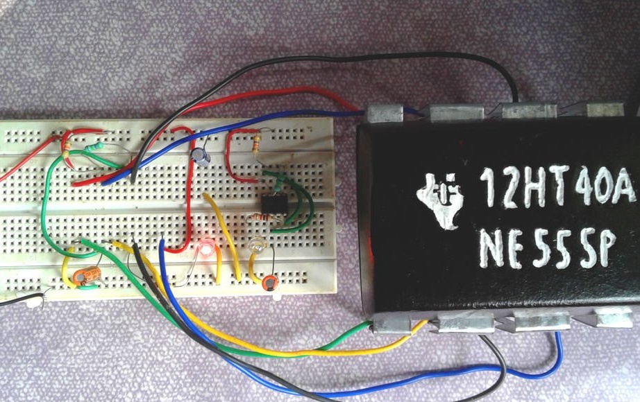
By debugging the circuit, YADUKRISHNAN K M swaps the flexible pin conductors with pins. Where the microcircuit has a notch, it makes a similar notch on the board. With pins, a functional analog can be put on a breadboard type board instead of the usual 555 timer and assemble the same circuits on it - they will work the same way. For instance:
Here are two power-parallel generators, one on a microcircuit, the other on a functional analogue:
Do not pay attention that they work asynchronously - the whole point is in the scatter of the parameters of resistors and capacitors. With two microcircuits, as well as with two functional analogs, the same thing would have happened.
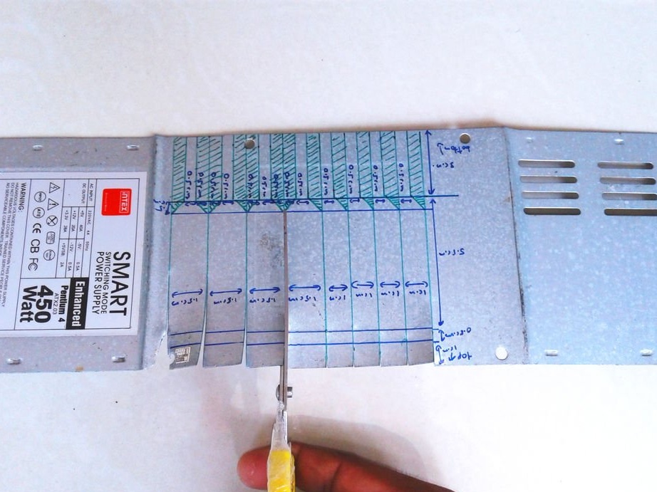
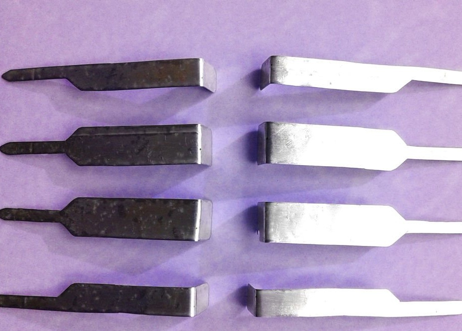
However, the master believes that differences in the threshold voltages of the comparators also make some contribution - they are such that the frequency with the same external elements is slightly higher. Now the master makes a case for a functional analogue in a scale of 10: 1. He draws conclusions from the case from a computer PSU. Marks:
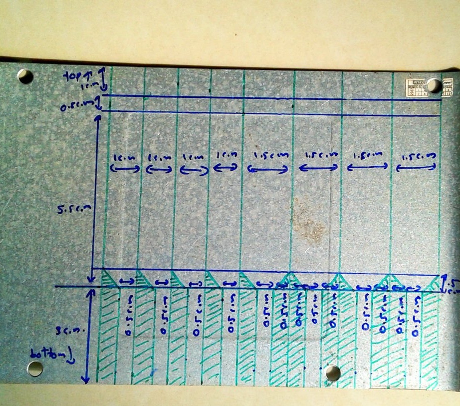
Cuts out:
Oppression:
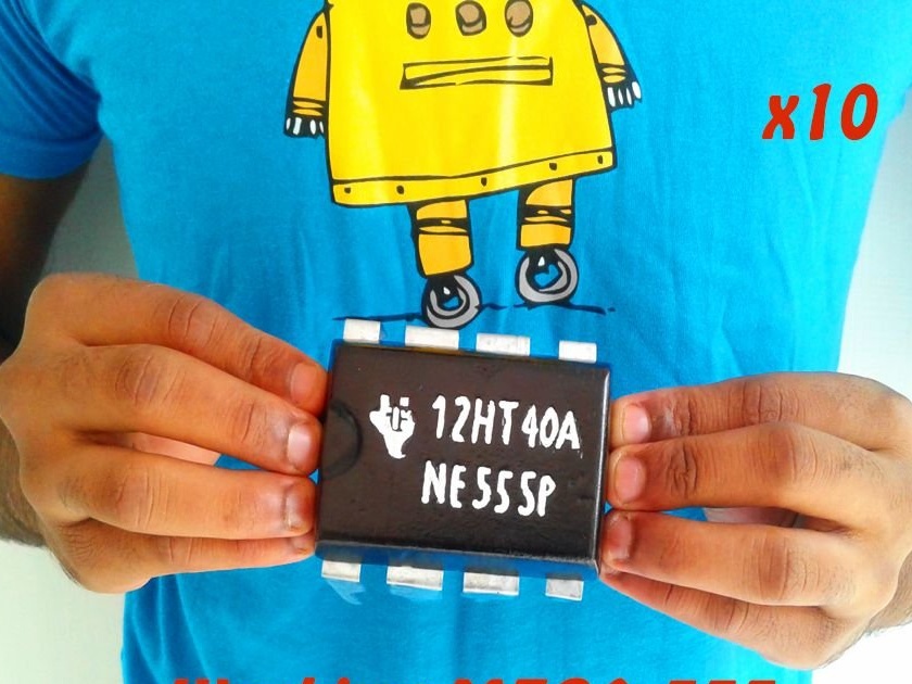
Like real ones!
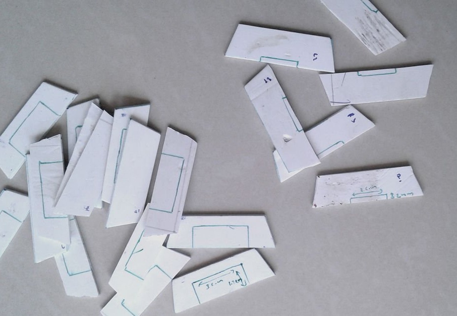
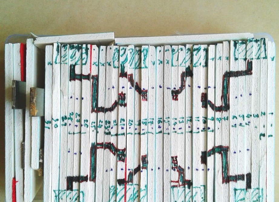
The master makes the case from old plastic plates for cabinets. Marks:
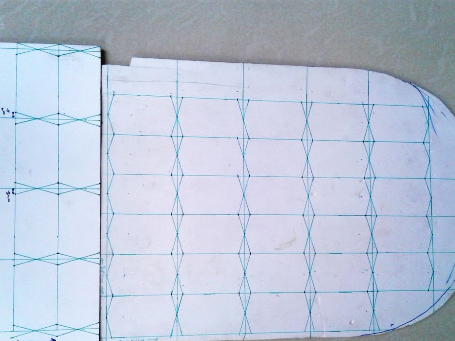
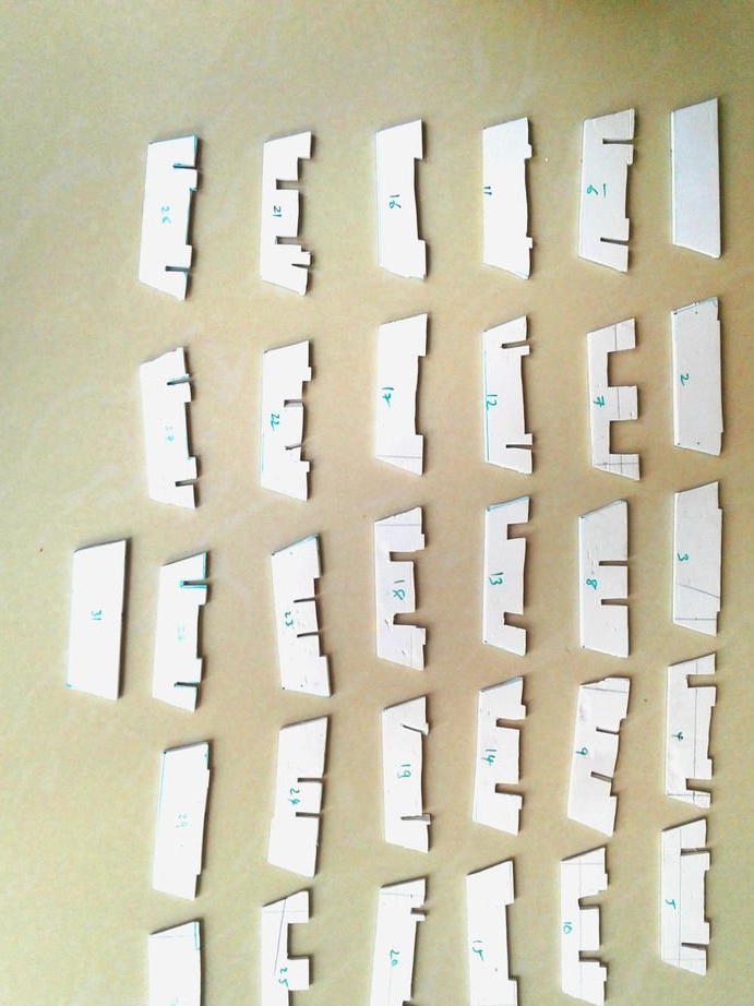
It cuts into many, many such pieces:
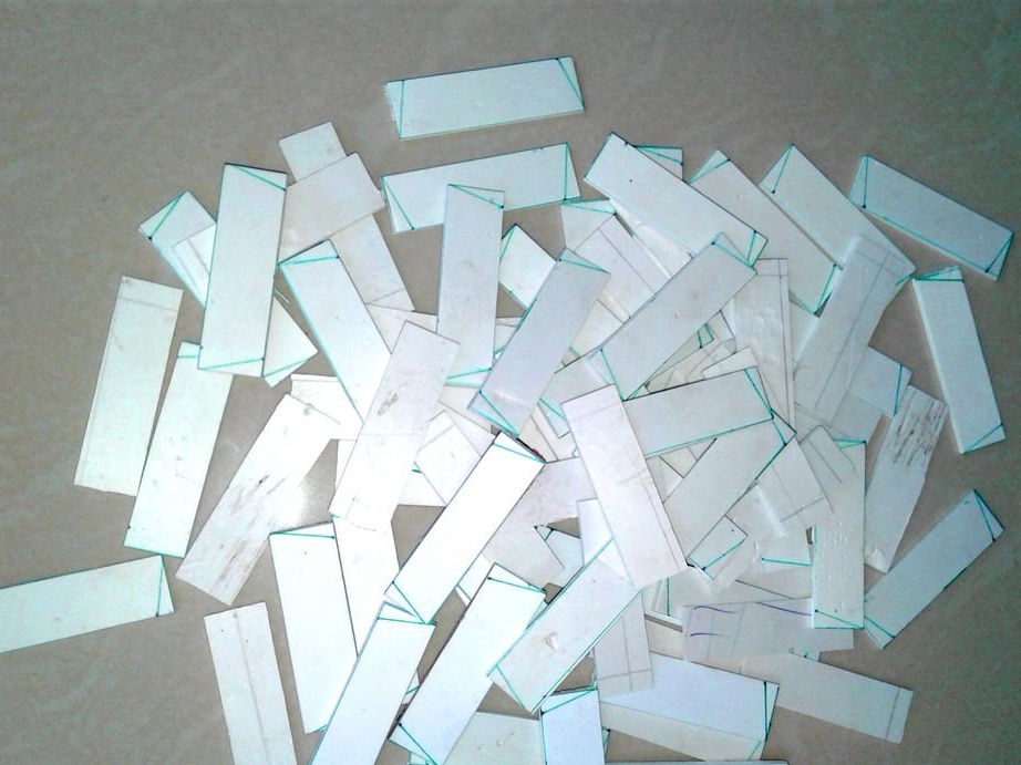
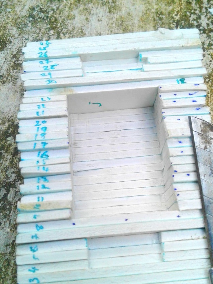
In some makes a notch:
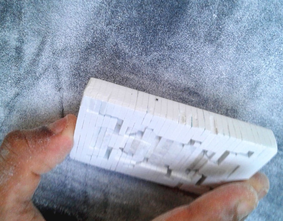
To then glue in layers in this:
After careful processing it turns out much more beautiful:
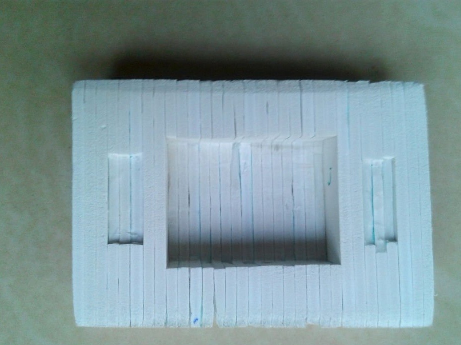
This is the upper half of the body, it is supposed to recess:
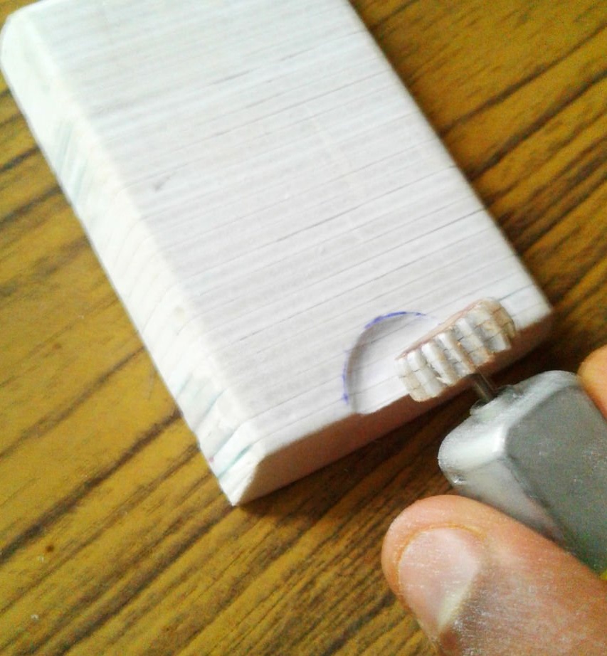
Bottom harder:
Here is what it will consist of:
And here is the result:
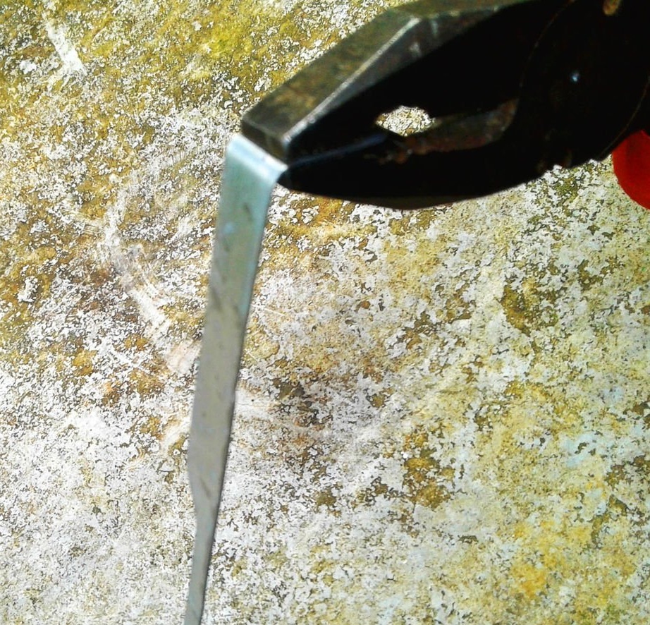
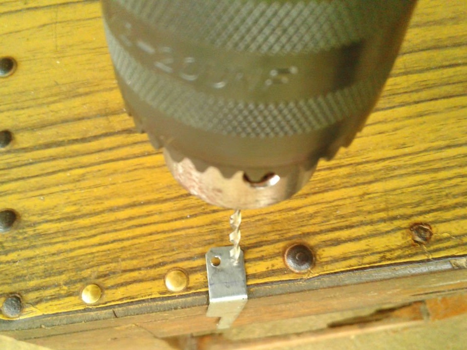
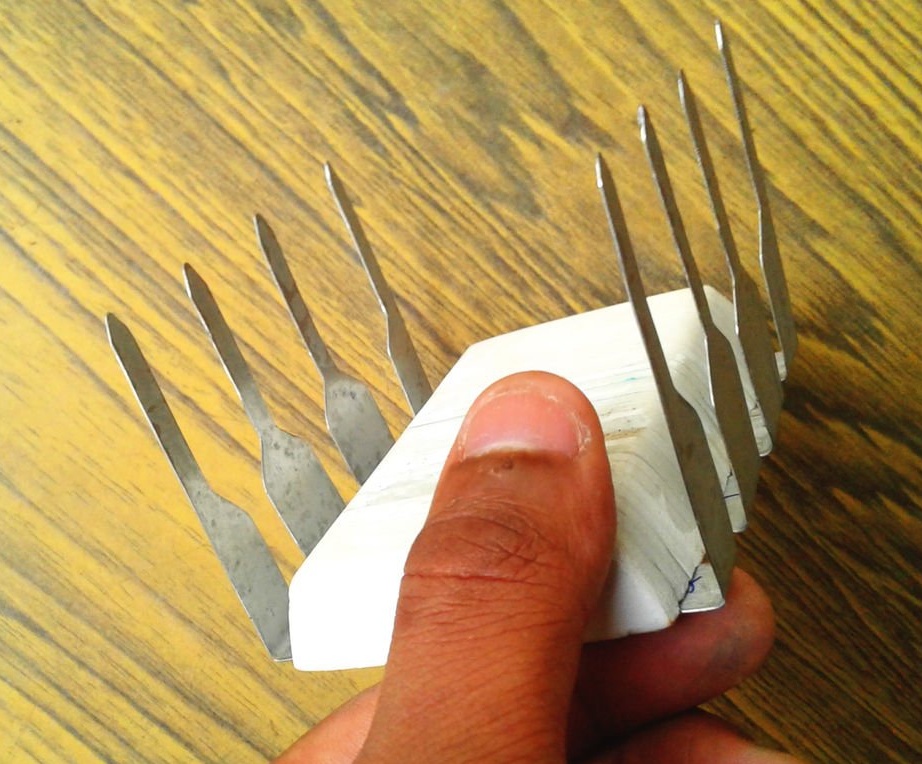
The master attaches the conclusions to it:
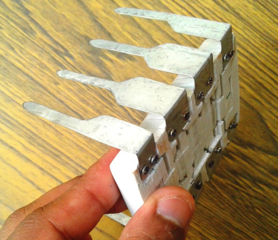
Having previously made the mounting holes in them:
Here is the result:
Having removed the conclusions, the master outputs wires from the board with long stripped and tinned ends. The board is placed in the lower half of the case, the wires through the recesses lead to the points of attachment of the terminals:
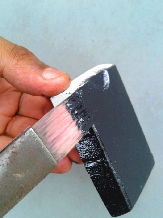
Paints half the body:
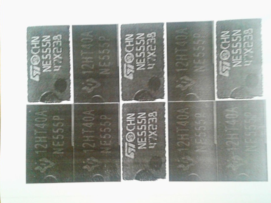
Photographs a microcircuit, prints a photo in a greatly enlarged form:
Makes a stencil:
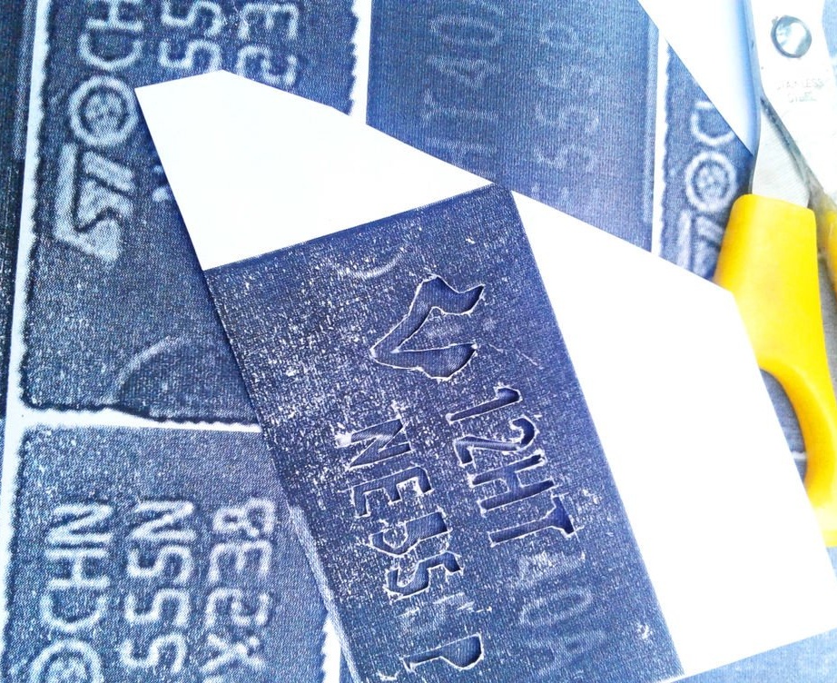
It engraves the upper half of the body:
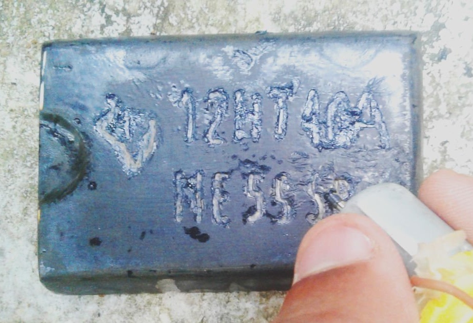
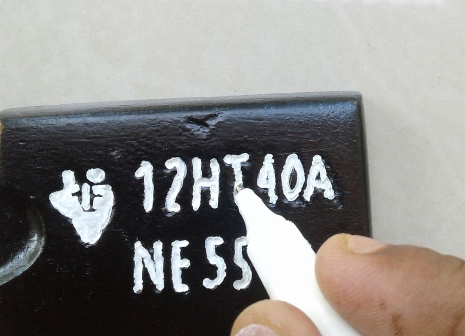
The engraving is filled with a “stroke” in two layers, the second one is applied after the first one has dried:
Do not want to take pictures yourself - download file for printing stencil.
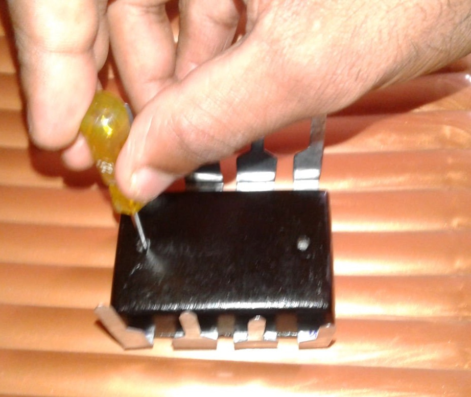
The master puts the conclusions in place, pressing them to the wires, and collects everything together:
Do not guess - not on glue. On the screws. If something breaks, you can fix it:
Checks again, and again everything works: