
This article is dedicated to quite powerful e load, which is useful for checking various power supplies.
This homemade product is especially useful for amateur radio amateurs, like Roman, the author of the YouTube channel “Open Frime TV”. Further instructions are taken from the aforementioned YouTube channel.
About a year has already passed since the author collected the load on the field effect transistor (a video about the assembly and tests is on the author’s channel).
At that time, there were absolutely no complaints about the device, and it completely satisfied the master. But progress nevertheless does not stand still and the power supply units are growing, this load is already not enough.
So the time has come to collect something more powerful. And since it’s more powerful, it is necessary to use not one transistor, but several at once, and the transistors should also be not field, but bipolar for operation in linear mode.

Well, there are drafts for the project, you can gradually proceed to the ego implementation. On the Internet there is simply a huge variety of electronic load schemes.

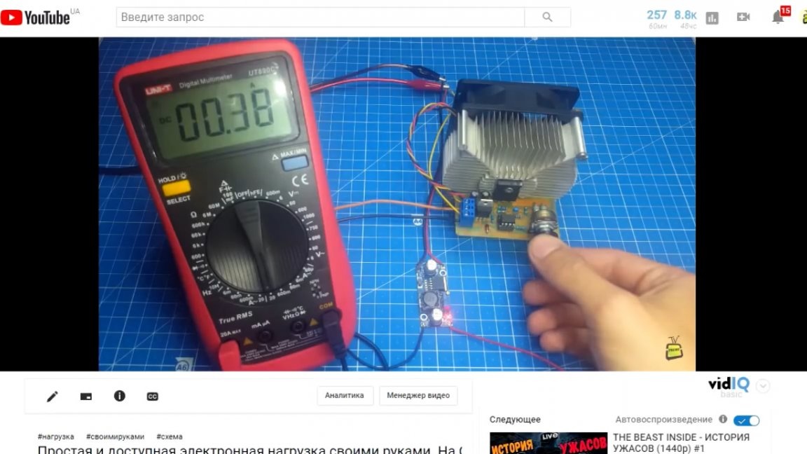
Which one to choose? The author did not spend much time solving this issue, and took as a basis the electronic load scheme from the YouTube channel “Red Shade”.

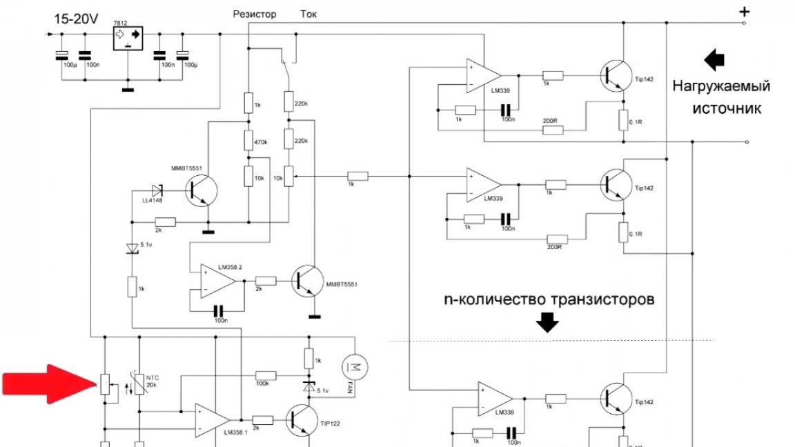
The scheme itself is excellent, but the decision on the board of the author of this project did not work, so I had to redo it for myself. So, the image below shows the load scheme itself:

So, let's figure out what is here and why. First of all, we look at the node responsible for stabilizing the current.
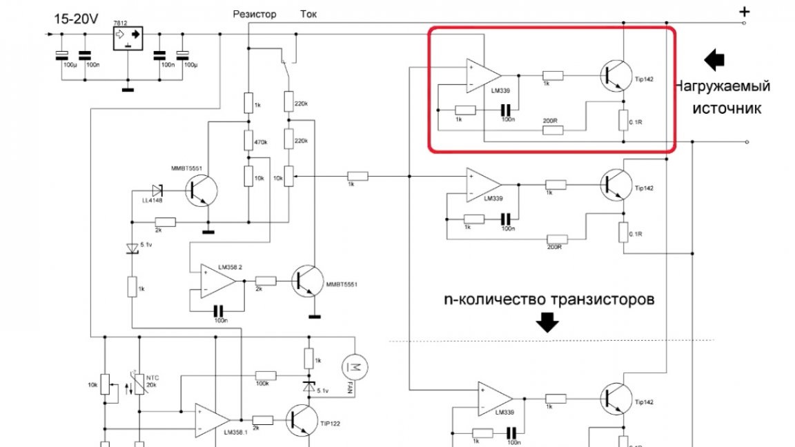
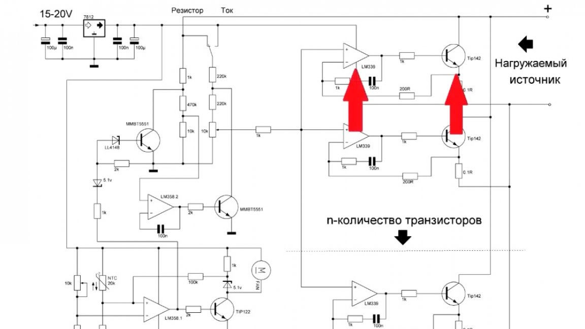
As you can see, here each transistor is equipped with its own operational amplifier. This solution gives us separate current control even if the transistors have parameters h21 different, there will be no current imbalance.
The next feature of the load is the ability to work in 2 modes. The first is the current mode.
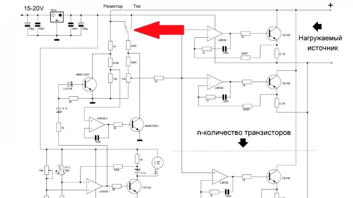
Everyone knows the mode when we set a specific current as a reference voltage, and whatever the input voltage of the loaded source, the current will be unchanged.

The second mode is the resistor mode.
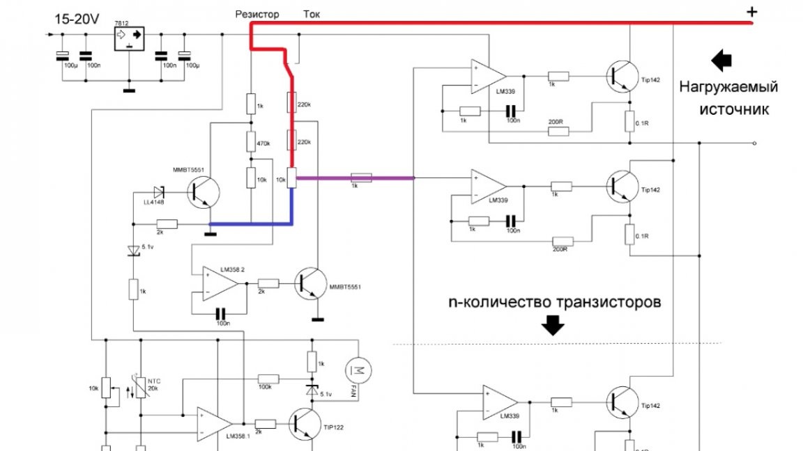
In this inclusion, the reference voltage is set by the input voltage.
It would seem, what is the purpose of this (second) mode? And the thing is that to check laboratory power supplies with the function of limiting the current, the first mode is not convenient to use, since the swing begins.
Current stabilization should be present in only one of the two devices, for this very reason the circuit contains 2 different operating modes.
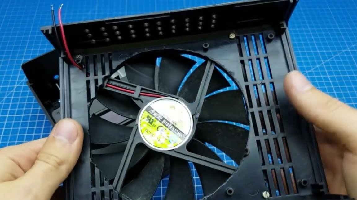
Move on. In this scheme, there are a couple more nice features. Firstly, it is an automatic control of the cooler for heating, which is quite convenient, since with the load off, the device will stand silently, without distracting you from extraneous noise. And as soon as the radiator temperature rises, the cooler will automatically turn on and thereby cool the circuit.
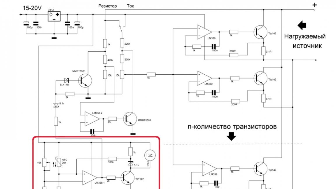
In addition to the above solution, the circuit also implements overheating protection. Definitely a useful thing.
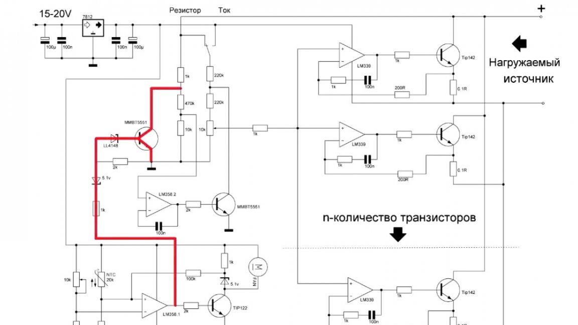
If you forget and leave the load unattended, you can be sure that it will disconnect itself if the temperature exceeds the set value.
The adjustment threshold for overheating protection is made by this tuning resistor:
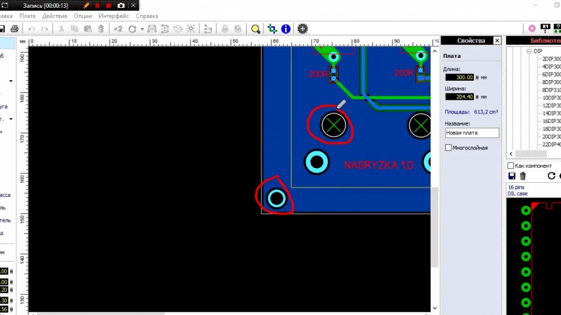
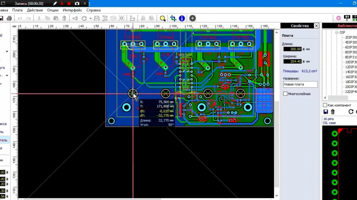
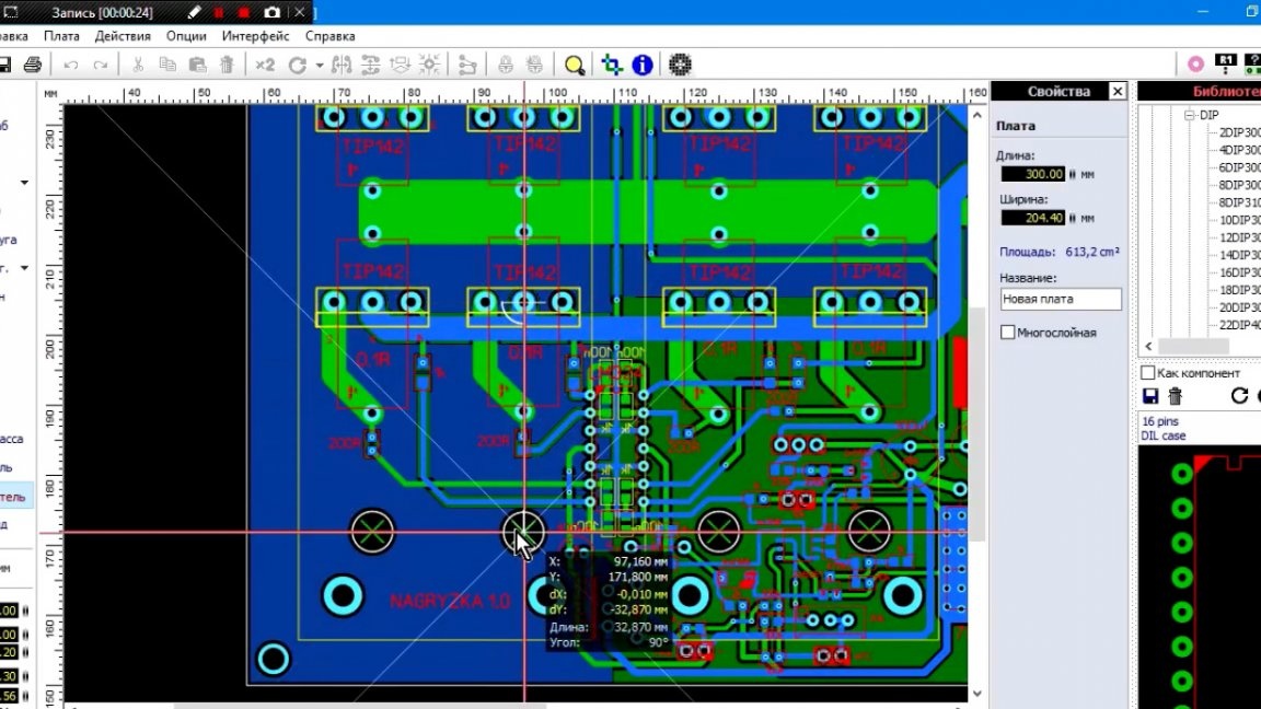
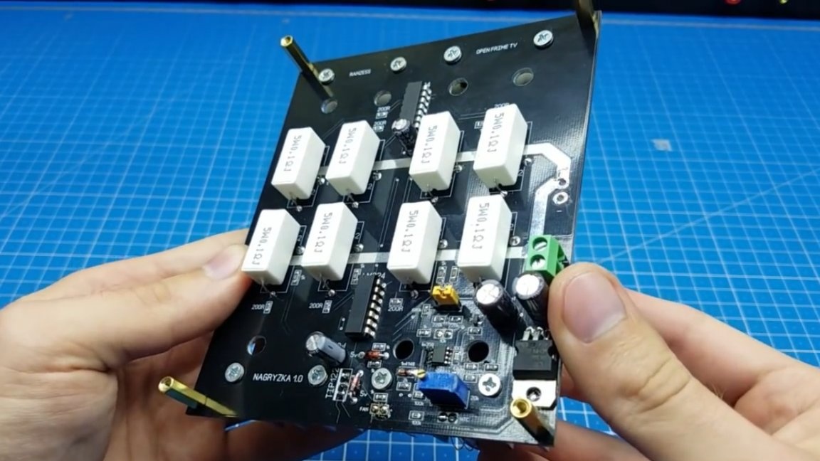
The next step - PCB trace.
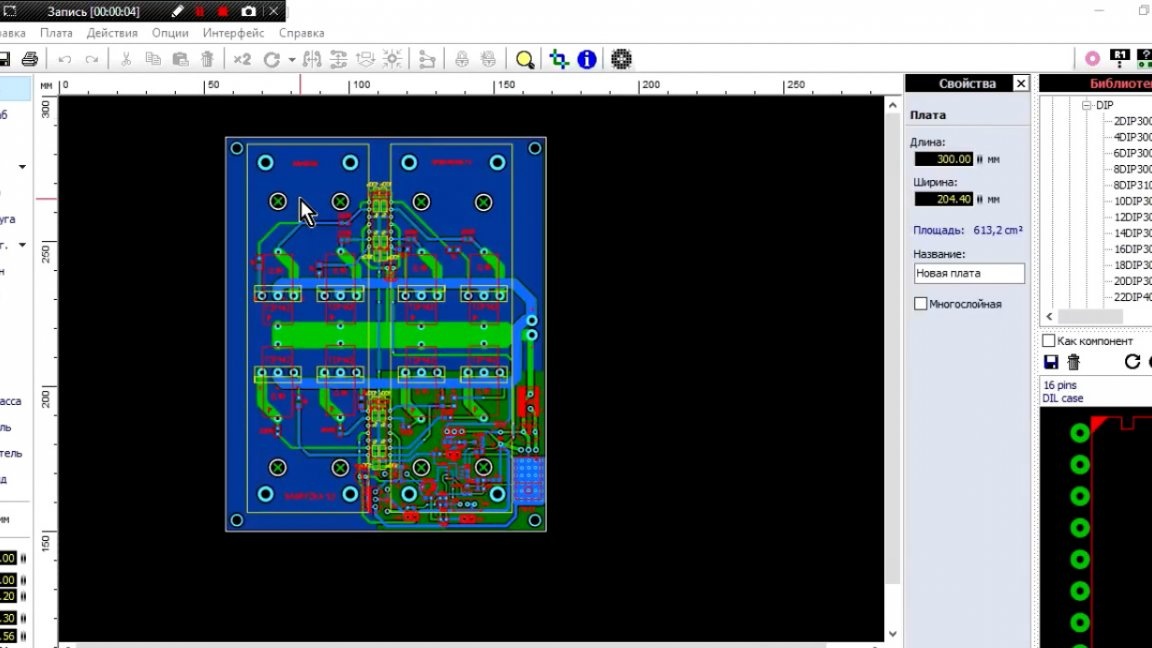
The author thought for a long time about how to make sure that all the elements were located on one printed circuit board. Ultimately, a solution was found. The author came up with the smart idea to arrange transistors as they do in welding machines. No sooner said than done, radiators with transistors are brought to the other side.
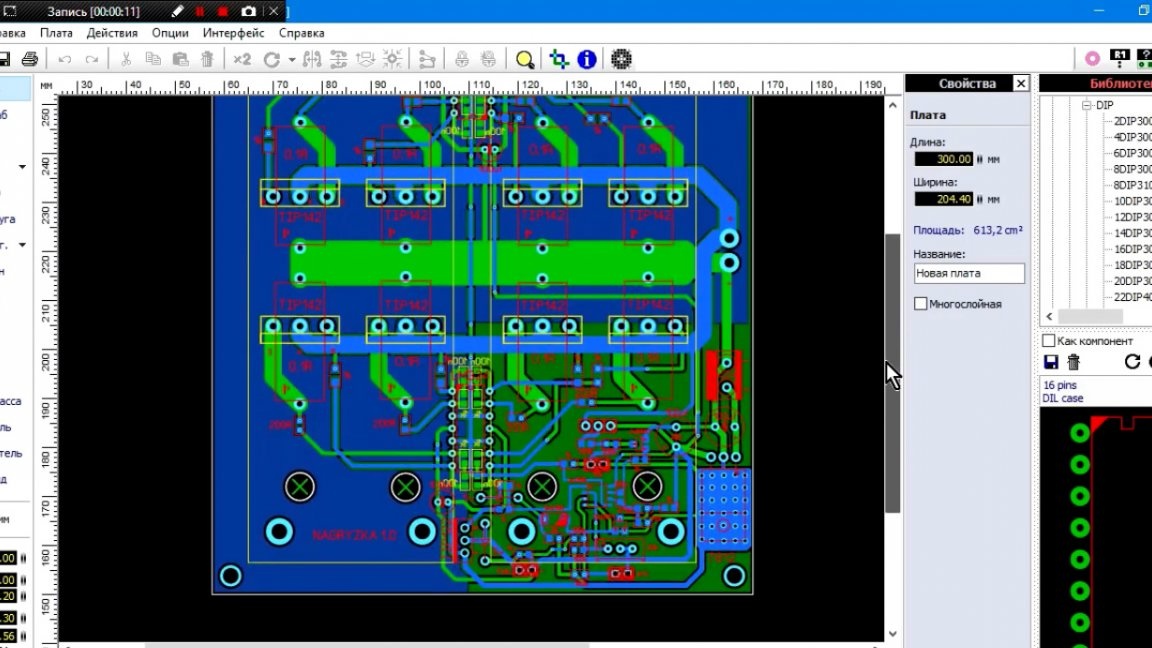
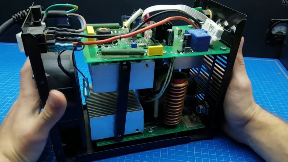
For more convenient mounting, special holes have been made for racks and one more for mounting transistors to the radiator:
At this stage, the author admits that he made a mistake, as he made holes for mounting the transistor very far from its actual location, so in the future he had to fix this joint.
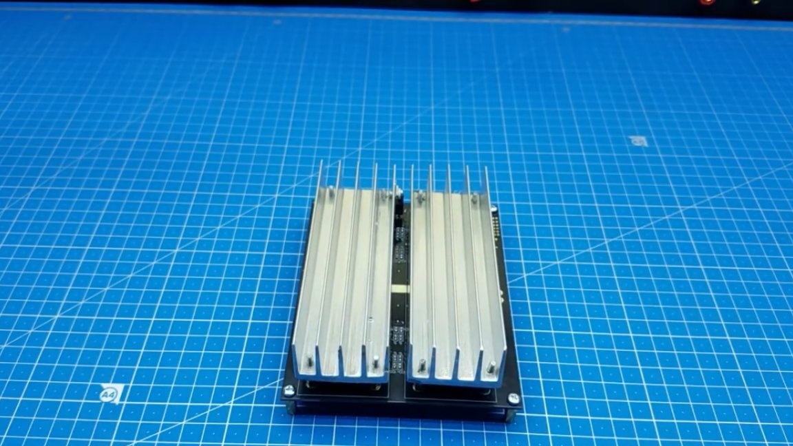
Here is the board:

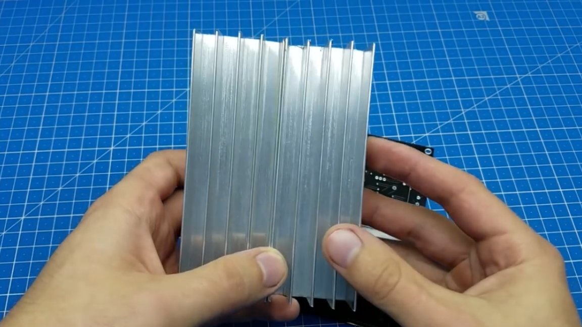
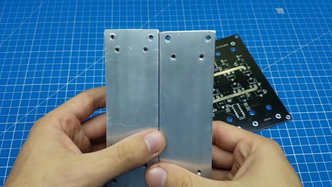
As radiators, it was decided to use an aluminum profile.
The first step is to cut it into two equal parts, and then drill holes for fasteners. Next, we cut the m3 thread and this is what happened in the end:
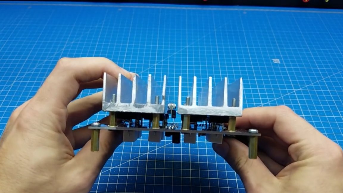
Next step fasten the transistors to the radiator.

Next, the resulting design should be assembled in one piece:

Using tenth racks, we gently connect the radiators to the board. Now they are definitely not going anywhere.
Due to the fact that the holes for mounting the transistor are not located where necessary, the repair of this board is very complicated. But let's be honest, burning this board will be very difficult, since 8 transistors can draw quite decent current through itself, and besides, overheating of the circuit is practically impossible, since the corresponding protection is present on the circuit.
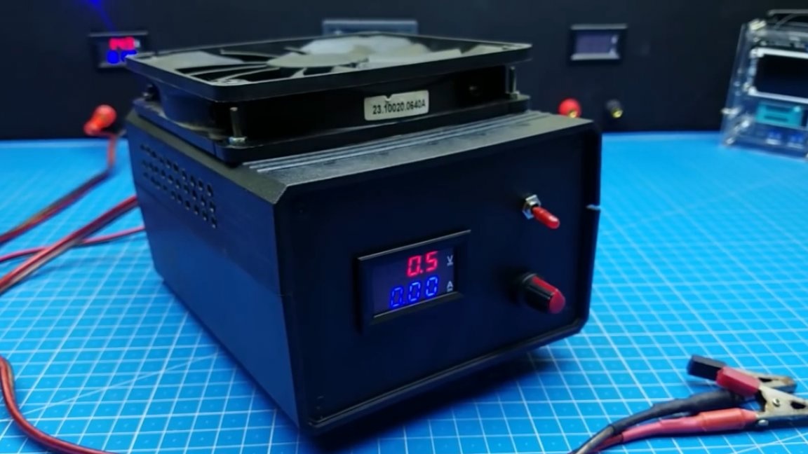
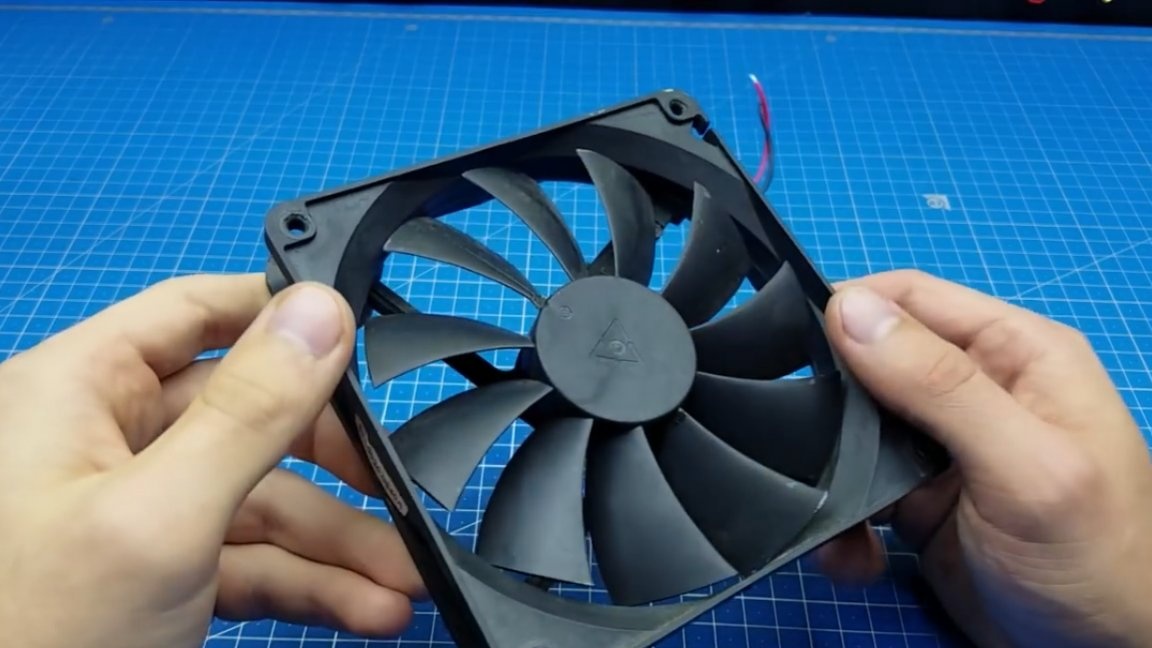
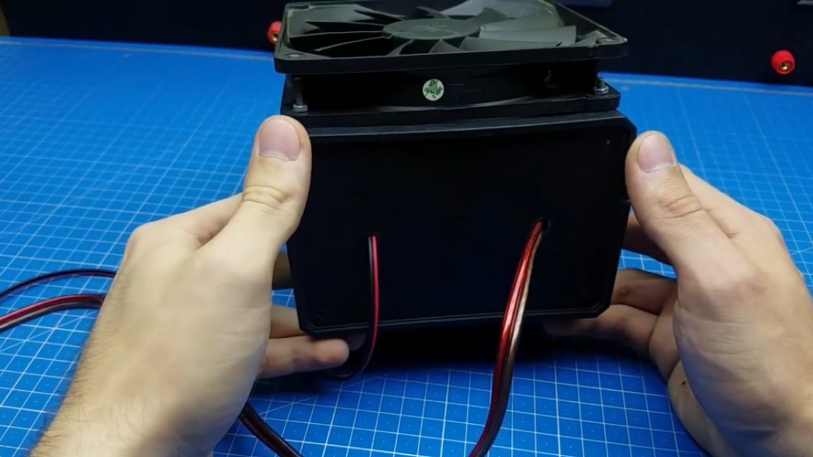
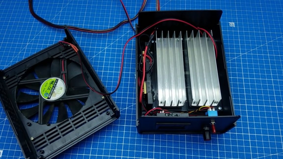
Next step it is necessary to select a suitable case for the load and place it there, since we make it as a finished device, which will then be used everywhere. Such a plastic box with rather convenient partitions came up perfectly as a case:

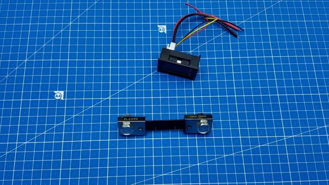
In addition to the direct load, it will also accommodate a couple of components, namely a voltammeter and a cooler.

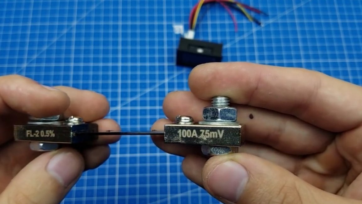
As you know, as standard, a multimeter allows you to measure current up to 10A. For this project, the author considered that this was not enough and to expand the measuring range, such a shunt was purchased that allows you to measure currents up to 100A:
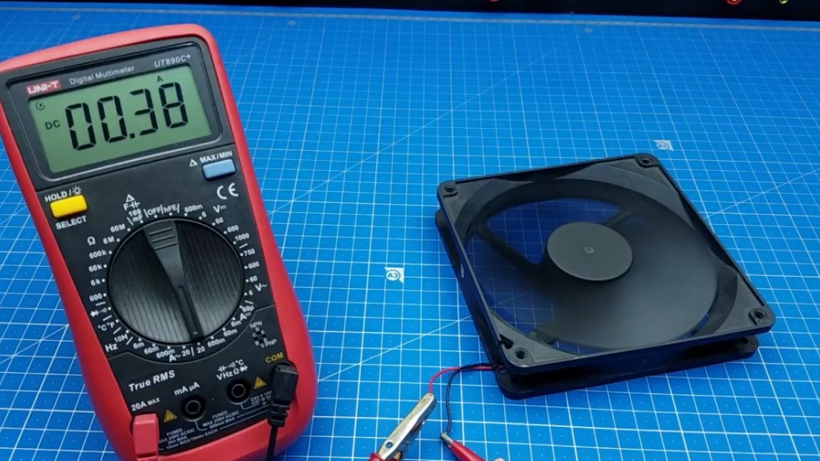
For this project, it was decided to use the 150th cooler, since it is able to create an excellent air flow due to the imposing blades, and this is extremely important for us. On the sticker of the cooler there is information that the current consumption of this instance can reach as much as 450mA.
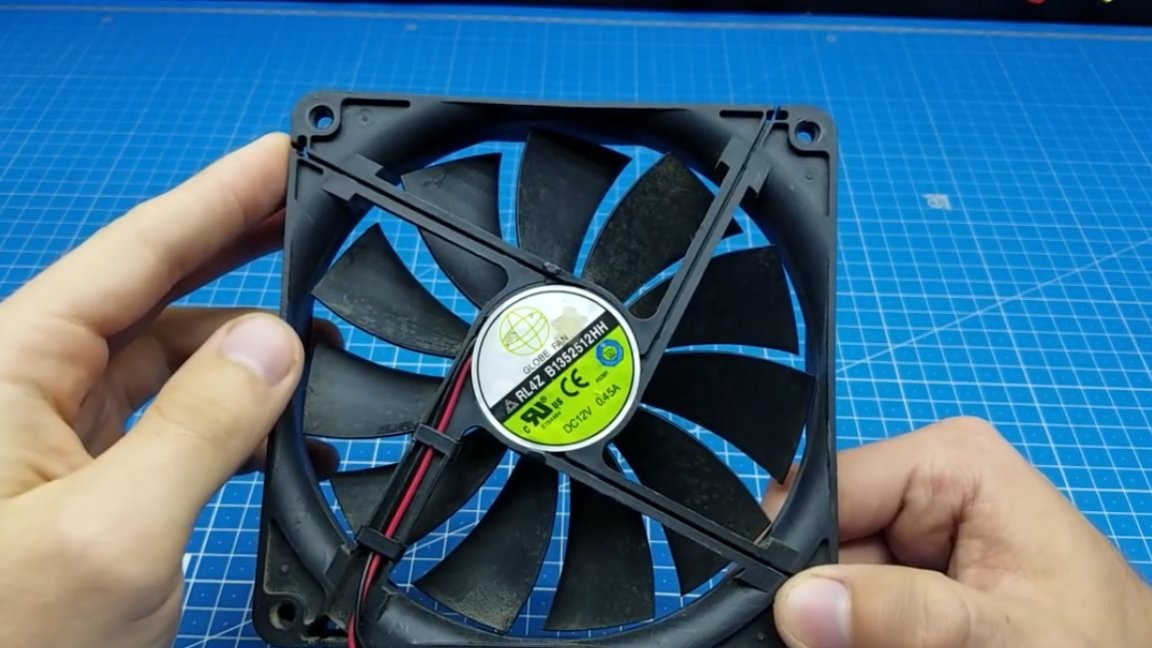
In reality, this value is a little less.
Next step proceed to marking the case, and then drill the necessary holes. The cooler had to be placed on top, since the overall dimensions of the case do not allow it to be placed inside.
On the front panel we place a multimeter, a current control knob and a current-resistor switch.

The power input and the load wire are located on the rear panel.

Next step we fix all the components in the case. A little hot glue will not be superfluous. This is how the device looks after installation in the case.
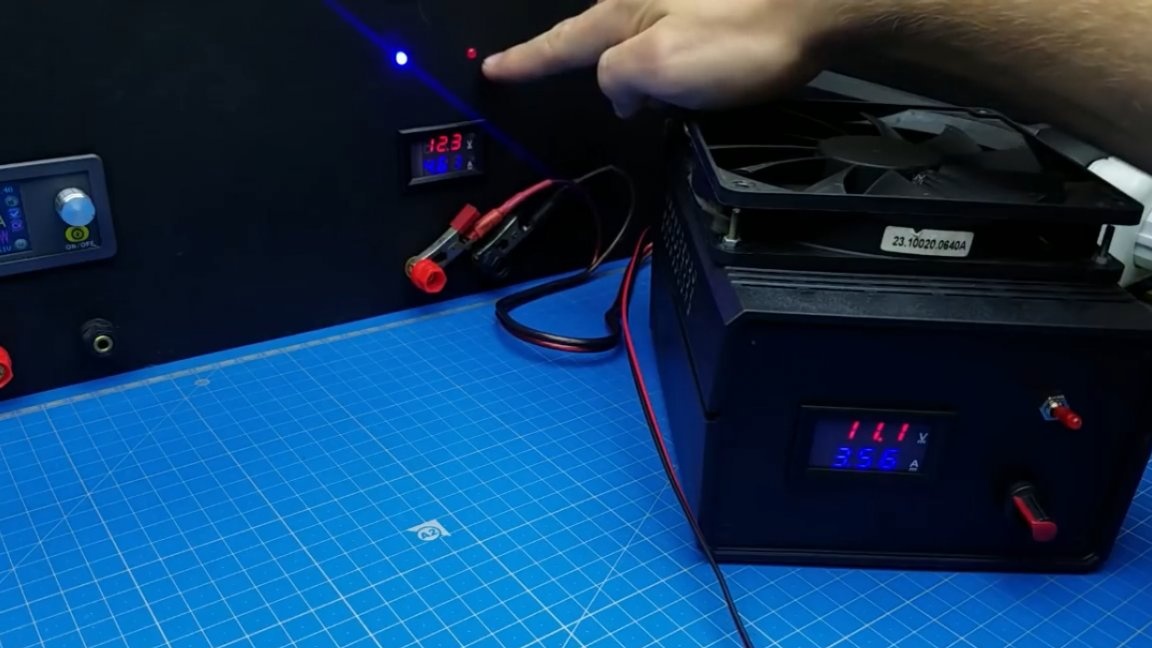
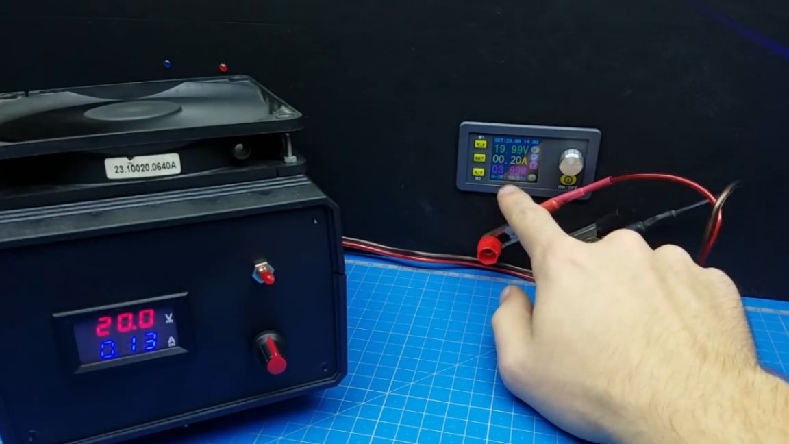
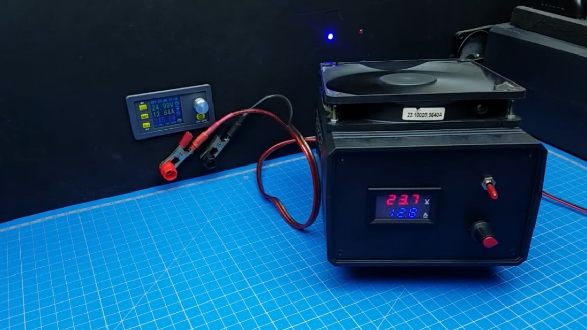
That's all, you can close the lid and proceed to the tests. Let's start the test with the DPS5020. Let's try to load this power supply.
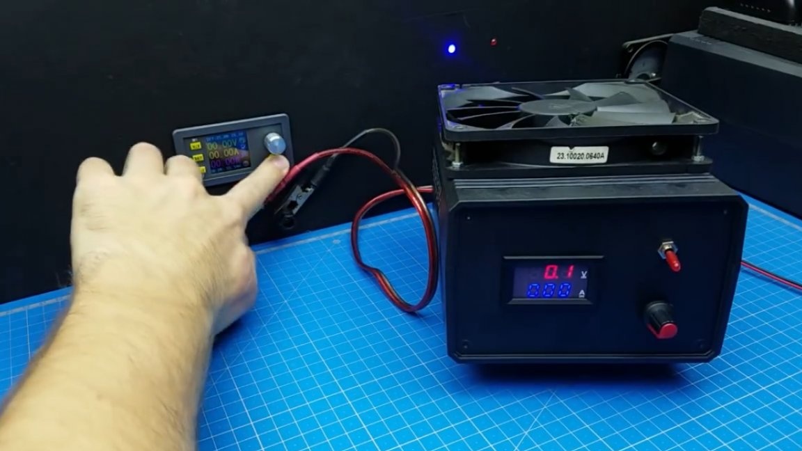
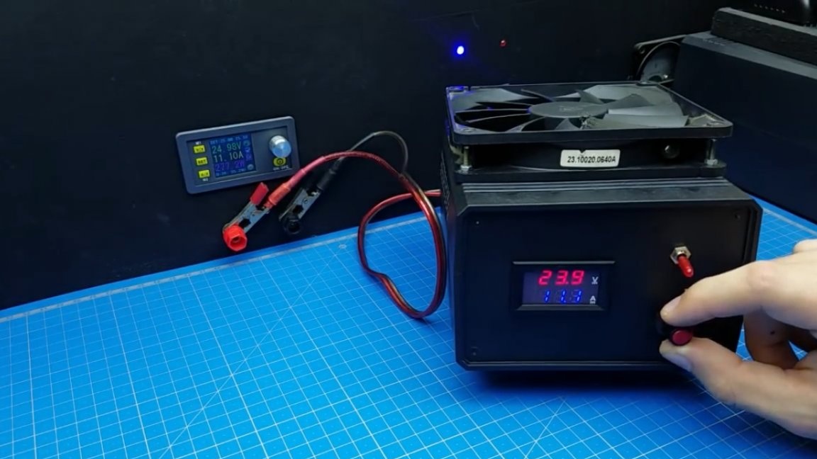
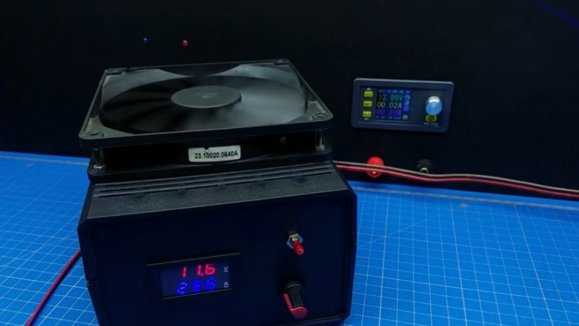
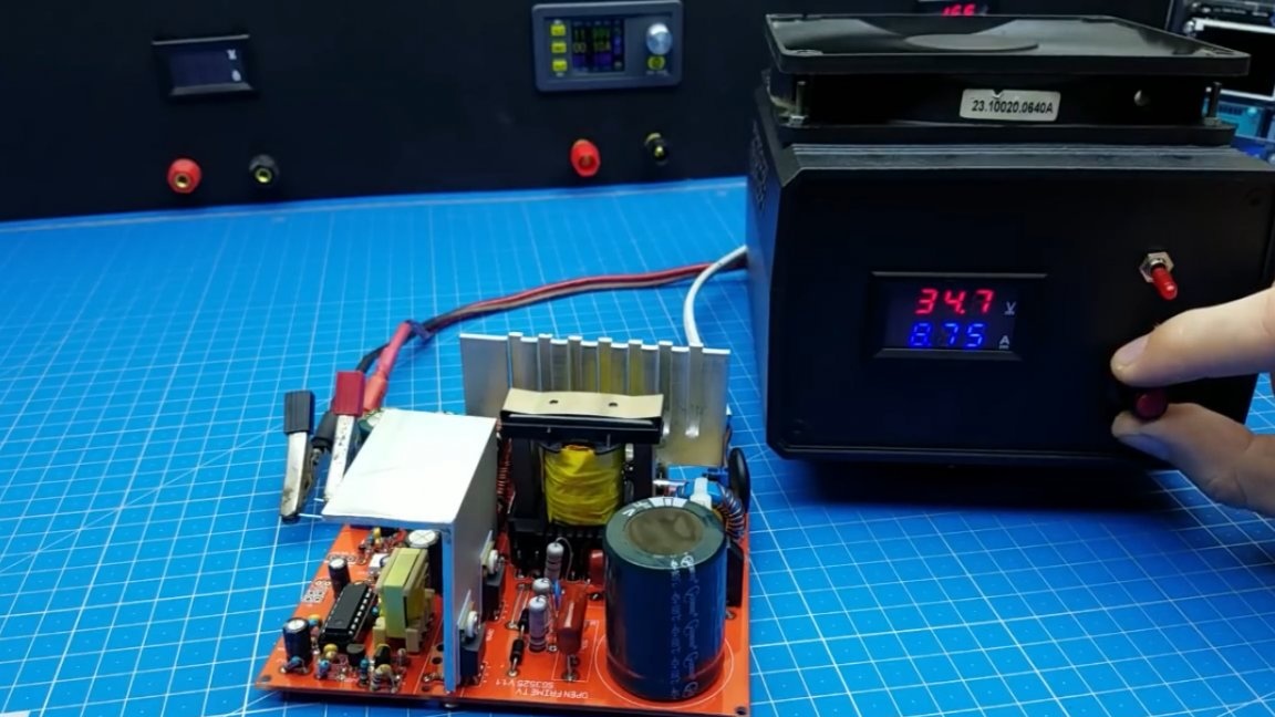
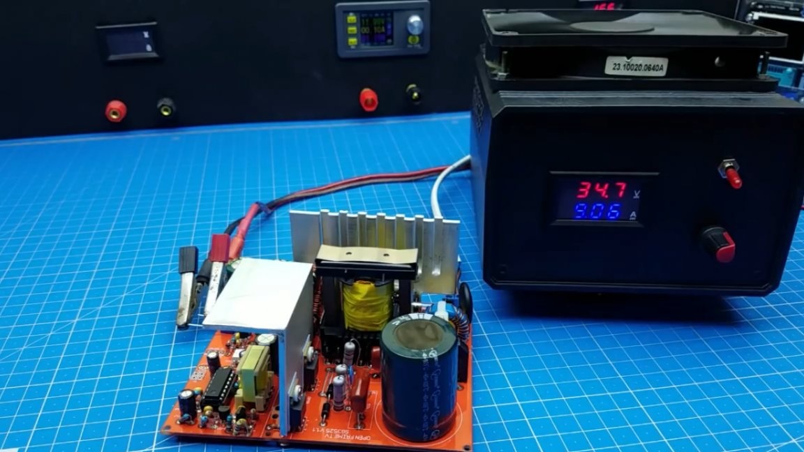
As you can see, the load copes perfectly, heating is within acceptable limits. Next, load the block on the SG3525.
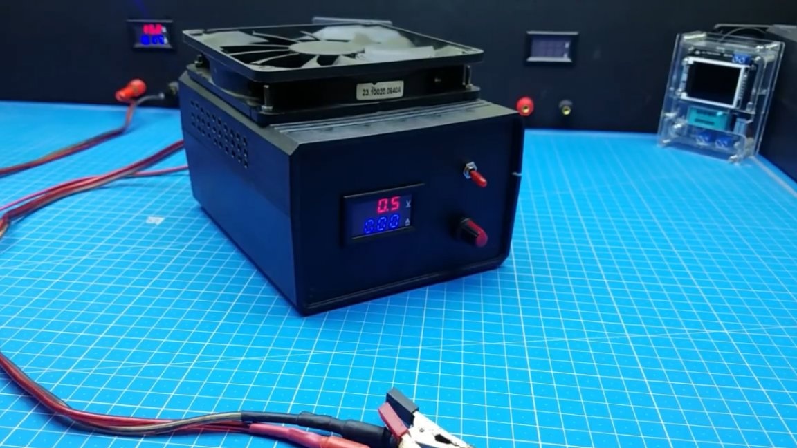
Everything is fine here too, the load successfully copes with the tasks. Here is a device in the end turned out. Thank you for attention. See you soon!
Author's video: