
It is possible that these experiments will later be presented on the Web and the cause will reconnect with the investigation in the most natural way. While it’s really different.
Electronics It is strong in recycling when parts of what has already been made are repeatedly used for completely different purposes. So use this device at least in whole, at least in parts, where its function is required. And she, as you see, is not standard. This can be background advertising, tricks, service bulletin boards of theater halls, etc., where distraction from some basic task destroys it.
Principle of operation
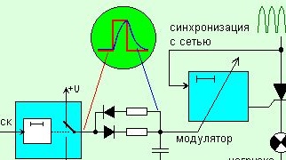
The luminous function is formed on the capacitor by the mode of its charge and discharge from the output of a single pulse generator and is supplied to the phase control modulator with a triac key. The key is powered by a rectified alternating voltage. Its fall to zero triggers a one-shot phase delay start of the seven-cell. The delay value depends on the voltage at the modulating input.
Work
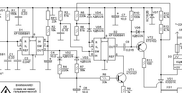
The generator of the highlighting function is assembled on the integrated timer chip D1. In the initial state, a high signal level at the input IL (pin 2) gives a low signal level at the output OUT (pin 3). The capacitor C6 is discharged along the circuit VD3, R7 open "lower" output transistor D1, common wire. When the SB1 "START" button is pressed at the input IL and the reset input R (pin 4), the voltage drops to zero, the internal trigger switches, and a high voltage level appears at the output. Capacitor C6 starts charging from the supply voltage through the opened "upper" transistor D1 timer output (pin 3) diode VD2, resistor R4.The end of the charge occurs with the end of the pulse at the output of the timer. The pulse duration depends on the charge time C2 from the supply voltage through the resistors R2 and RP1 to the level of 2 / 3Upit. This level is monitored at the input of IH (pin 6). By the signal from the button, it generates one pulse of negative polarity at the output (OUT pin 3). The formation of the analog signal of the desired shape is carried out on the capacitor C6, which is charged and discharged from the output of the timer through resistors R4 and R7. Separation of charge and discharge currents is carried out by diodes VD2 and VD3.
The received analog half-wave signal is fed through VT1 to the input of timer D2 (REF pin 5). In this case, VT1 is turned on as a controlled current load, which shunts the lower resistor of the timer reference divider. In this case, the effect of modulation of the function performed by him arises.
Replacements
D1, D2 integrated timers.
They are replaced by any analogue of the NE555 grandparent, both bipolar and CMOS (NE7555), for example, domestic KR1441VI1. The analogues of the dual timers NE556 and NE7556 are economical, since the price for one timer in this case is one third lower.
VT1, VT2 transistors.
There are no special requirements for them and use any low-power transistors of the corresponding structures at these positions.
VD1 ... VD6 diodes.
These are any low-current diodes.
VS1 triac.
Use KU201I ... M, KU202K ... M, T122-10 -...
D3 diode bridge.
It is possible to replace it with a classic bridge of four separate diodes with a working current of 1A, pulse up to 10A and a reverse voltage of 400V. The large requirements for pulsed current are due to work on incandescent lamps, which have a cold resistance of a tungsten filament ten times lower than in a red-hot one.
Advice
The device was manufactured in only three, somewhat different circuit models, on prototyping boards and printing was not developed.
For your own safety, place live parts separately from the controls. This applies to R11 ... R13, VS1, D3, FU1, XS1.
It is rational to carry out repair and adjustment of the device from a laboratory power supply with a voltage of 8 ... 10V set on it, connected to VD6 through an additional 750 Ohm resistor.
Evg. Fistula